Industry News | 2018-10-18 10:24:05.0
The Design Principles of Stencil Apertures
Industry News | 2018-10-18 11:08:57.0
What are PCB Thickness Options?
Industry News | 2018-10-18 11:19:07.0
How To Design Cost-Effective PCBs
Industry News | 2018-12-08 03:29:29.0
SMT Dictionary – Surface Mount Technology Acronym and Abbreviation
Technical Library | 2015-08-27 15:32:16.0
Ever since there has been a widespread usage of surface mount parts, the trend of continued shrinkage of devices with ever finer pitches has continued to challenge PCB assemblers for the rework of same. Todays' pitches are commonly 0.5 to 0.4mm with packages of tiny outline sizes, 5 -10mm square, making the rework of such devices a challenge. In addition to the handling and inspection challenges comes the board density. Spacing to neighboring components continues to be compressed so the rework techniques should not damage neighboring components.
Technical Library | 2017-09-28 16:36:33.0
These nano-coatings also refine the solder paste brick shape giving improved print definition. These two benefits combine to help the solder paste printing process produce an adequate amount of solder paste in the correct position on the circuit board pads. Today, stencil aperture area ratios from 0.66 down to 0.40 are commonly used and make paste printing a challenge. This paper presents data on small area ratio printing for component designs including 01005 Imperial (0402 metric) and smaller 03015 metric and 0201 metric chip components and 0.3 mm and 0.4 mm pitch micro BGAs.
Technical Library | 2015-12-31 15:19:28.0
Today's consumer electronic product are characterized by miniatuization, portability and light weight with high performance, especially for 3G mobile products. In the future more fine pitch CSPs (0.4mm) component will be required. However, the product reliability has been a big challenge with the fine pitch CSP. Firstly, the fine pitch CSPs are with smaller solder balls of 0.25mm diameter or even smaller. The small solder ball and pad size do weaken the solder connection and the adhesion of the pad and substrate, thus the pad will peel off easily from the PCB substrate. In addition, miniature solder joint reduce the strength during mechanical vibration, thermal shock, fatigue failure, etc. Secondly, applying sufficient solder paste evenly on the small pad of the CSP is difficult because stencil opening is only 0.25mm or less. This issue can be solved using the high end type of stencil such as Electroforming which will increase the cost.
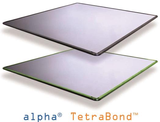
New Equipment | Solder Paste Stencils
ALPHA® Stencil products are based on unique blends of advanced technology, the experience gained from having made over half a million solder paste stencils, the specialist knowledge that could only be accumulated by a company privileged to produce bo
.gif)


