Welwyn Components� new SMT facility contains the latest manufacturing techniques for both standard and specialist chip resistors. These include high speed/ high precision printing and lasering equipment, grading and tape packing machines and a state
Technical Library | 2023-07-25 16:50:02.0
Some of the new handheld communication devices offer real challenges to the paste printing process. Normally, there are very small devices like 01005 chip components as well as 0.3 mm pitch uBGA along with other devices that require higher deposits of solder paste. Surface mount connectors or RF shields with coplanarity issues fall into this category. Aperture sizes for the small devices require a stencil thickness in the 50 to 75 um (2-3 mils) range for effective paste transfer whereas the RF shield and SMT connector would like at least 150 um (6 mils) paste height. Spacing is too small to use normal step stencils. This paper will explore a different type of step stencil for this application; a "Two-Print Stencil Process" step stencil. Here is a brief description of a "Two-Print Stencil Process". A 50 to 75 um (2-3 mils) stencil is used to print solder paste for the 01005, 0.3 mm pitch uBGA and other fine pitch components. While this paste is still wet a second in-line stencil printer is used to print all other components using a second thicker stencil. This second stencil has relief pockets on the contact side of the stencil any paste was printed with the first stencil. Design guidelines for minimum keep-out distances between the relief step, the fine pitch apertures, and the RF Shields apertures as well relief pocket height clearance of the paste printed by the first print stencil will be provided.
Industry Directory | Consultant / Service Provider / Manufacturer
Metal Etch Services is a manufacturer of Laser Cut Stencils, Thick Film Printing Screens, Metal Masks and Thin Metal Parts.
Technical Library | 2023-07-25 16:42:54.0
Printing solder paste for very small components like .3mm pitch CSP's and 01005 Chip Components is a challenge for the printing process when other larger components like RF shields, SMT Connectors, and large chip or resistor components are also present on the PCB. The smaller components require a stencil thickness typically of 3 mils (75u) to keep the Area Ratio greater than .55 for good paste transfer efficiency. The larger components require either more solder paste height or volume, thus a stencil thickness in the range of 4 to 5 mils (100 to 125u). This paper will explore two stencil solutions to solve this dilemma. The first is a "Two Print Stencil" option where the small component apertures are printed with a thin stencil and the larger components with a thicker stencil with relief pockets for the first print. Successful prints with Keep-Outs as small as 15 mils (400u) will be demonstrated. The second solution is a stencil technology that will provide good paste transfer efficiency for Area Ratio's below .5. In this case a thicker stencil can be utilized to print all components. Paste transfer results for several different stencil types including Laser-Cut Fine Grain stainless steel, Laser-Cut stainless steel with and w/o PTFE Teflon coating, AMTX E-FAB with and w/o PTFE coating for Area Ratios ranging from .4 up to .69.
New Equipment | Solder Paste Stencils
Laser Cut Stencils: Industry trend toward miniaturization is leading to finer pitch requirements, high tolerances, and greater repeatability. Our state-of-the-art laser technology enables our customers to experience positional accuracy unattainable w
New Equipment | Solder Paste Stencils
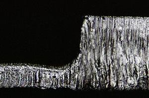
Through the increase of mixed technologies, stepped stencils have gained importance to the electronic assembly manufacturer. If the solder paste quantity can no longer be adequately regulated by adjusting Step/Relief Stencil Picture the pad sizes, st
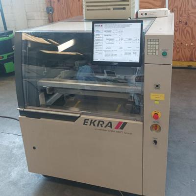
Used SMT Equipment | Screen Printers
EKRA X6 Screen and Stencil Printer Year: 2006 Reconditioned, in perfect working order. Automatic In-Line Stencil printer with steel welded frame; Two independent pneumatic Print Heads; EVA™ vision system with 2 cameras; Side and Top Clam
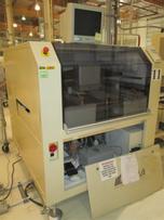
Used SMT Equipment | Screen Printers
Full 20" Conveyor width 2.5 D Inspection PCB Size: Min 80x50mm, Max 550x550mm, Thickness 0,5-6mm Stencil Size: 320x320mm up to 850x1000mm Contact me for more info, or visit our site at http://www.qcareelectronics.com/
BEST IPC J-STD-001 Revision F training kits feature REAL circuit boards that represent actual soldering conditions. This kit features "062 thick multilayer boards which are more representative of the thermal conditions of "real" circuit boards. This
Industry Directory | Manufacturer
Supplier of High-Tech Low-Cost Printed Circuit Boards with 1-48 layers from 24h express. Flex, flex-rigid, metal core, impedance control, blind & buried vias as well as SMD Stencils.


