Supplier: Shenzhen Grande Electronic Layers: 4 Application: General Industrial Equipment PCB Prototype/ China HASL PCB Manufacturer PCB Parameter: FR-4/HTG150 Thickness: 1.6mm Surface Treatment: HASL Testing: 100% E-test Package: Vacuum packing Lead
Supplier: Shenzhen Grande Electronics Layers: 4 Application: Stone Crusher PCB Prototype and Manufacturing Process | Grande PCB & PCBA PCB Parameter: FR-4/HTG150 Thickness: 1.6mm Surface Treatment: ENIG Testing: 100% E-test Package: Vacuum packing L
New Equipment | Board Handling - Pallets,Carriers,Fixtures
Supplier: Shenzhen Grande Electronics Layers: 4 Application: Grande - Automobile PCB Prototyping and Manufacturing PCB Parameter: FR-4/HTG150 Thickness: 1.6mm Surface Treatment: ENIG Testing: 100% E-test Package: Vacuum packing Lead Time: 10-15 da
Supplier: Shenzhen Grande Electronic Layers: 4 Application: Welding Machine Immersion Gold PCB Prototype / PCB Manufacturer China PCB Parameter: FR-4/HTG150 Thickness:1.6mm Surface Treatment: Immersion Gold Testing: 100% E-test Package: Vacuum packi

New Equipment | Board Handling - Storage
Supplier: Grande Electronics Layers: 4 Application: Pager Electronic Manufacturing | Fusion PCB Fabrication & Prototype PCB Parameter: FR-4/HTG150 Thickness: 1.6mm Surface Treatment: ENIG Testing: 100% E-test Package: Vacuum packing Lead Time: 10-15
New Equipment | Board Handling - Pallets,Carriers,Fixtures
Supplier: Grande Layers: 4 Application: Asset Tracking Device and System Turnkey PCB Solution - Printed Circuit Board Manufacturer PCB Parameter: FR-4/HTG150 Thickness: 1.6mm Surface Treatment: HASL Testing: 100% E-test Package: Vacuum packing Lead
Used SMT Equipment | In-Circuit Testers
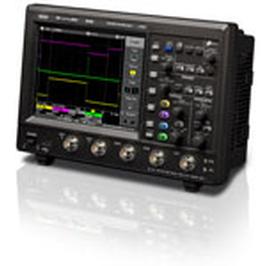
Teledyne LeCroy WaveJet 312A Bandwidth: 100 Mhz Channels: 2 100 MHz, 1 GS/s, 2ch, 500 kpts/Ch DSO with 7.5" Color Display. WaveJet 300A Oscilloscopes The WaveJet 300A provides the banner specifications, feature set and user interface to simplif
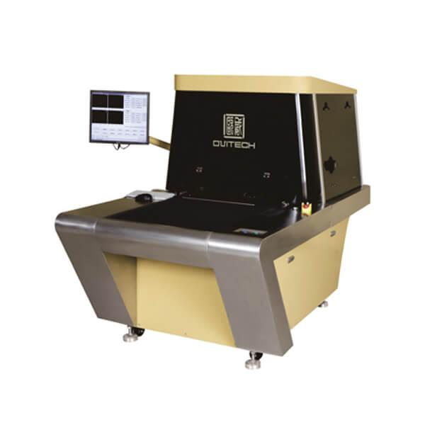
PCB Testing PCB circuit Quality Insepction Machine AOI T11 Scanning:face/hour 200 face 180face 160face 120face Test method based on size:18″×24″ 5mil 4mil 3mil 2mil Demension:2150mm×1350mm×1780mm Weight:1500KG Pr
Industry News | 2019-11-05 22:26:14.0
The board stack-up is probably the most essential piece for ensuring a successful PCB design. Modern high-speed boards require controlled-impedance traces, and whether you are using a simulation tool, a simple calculator, or the back of a napkin, you need to understand your manufacturing process to correlate your impedance calculations. This ensures that your trace widths and dielectric heights match what will actually be manufactured, and eliminates last-minute design changes.

PCB Testing PCB circuit Quality Insepction Machine AOI T11 Scanning:face/hour 200 face 180face 160face 120face Test method based on size:18″×24″ 5mil 4mil 3mil 2mil Demension:2150mm×1350mm×1780mm Weight:1500KG Pro


