Industry News | 2019-11-05 22:08:21.0
Via in pad is the design practice of placing a via in the copper landing pad of a component. Compared to standard PCB via routing, via in pad allows a design to use smaller component pitch sizes and further reduce the PCBs overall size. With component manufactures pushing smaller parts every year and the demand from consumers for smaller devices, the usage of via in pad practices by hardware engineers have become more commonplace. In this article, we will discuss the differences between via in pad and traditional vias, when should you use via in pad, and how to design for it.
Training Courses | | | IPC-600 Specialist (CIS)
The Certified IPC-600 Specialist (CIS) training targets quality assurance and acceptance of bare printed circuit boards.
Training Courses | | | IPC-600 Trainer (CIT)
The Certified IPC-600 Trainer (CIT) courses recognize individuals as qualified trainers in the area of quality assurance of bare printed circuit boards and prepare them to deliver Certified IPC-600 (CIS) training.
Training Courses | | | IPC-600 Trainer (CIT) Recert.
The Certified IPC-600 Instructor (CIT) recertification courses are intended for those individuals who were previously accredited to provide Certified IPC A 600 Specialist (CIS) courses.
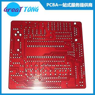
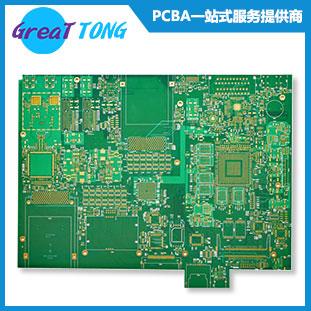
Supplier: Shenzhen Grande Electronic Layers: 4 Application: General Industrial Equipment PCB Prototype/ China HASL PCB Manufacturer PCB Parameter: FR-4/HTG150 Thickness: 1.6mm Surface Treatment: HASL Testing: 100% E-test Package: Vacuum packing Lead
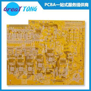
Supplier: Shenzhen Grande Electronics Layers: 4 Application: Stone Crusher PCB Prototype and Manufacturing Process | Grande PCB & PCBA PCB Parameter: FR-4/HTG150 Thickness: 1.6mm Surface Treatment: ENIG Testing: 100% E-test Package: Vacuum packing L
New Equipment | Board Handling - Pallets,Carriers,Fixtures
Supplier: Shenzhen Grande Electronics Layers: 4 Application: Grande - Automobile PCB Prototyping and Manufacturing PCB Parameter: FR-4/HTG150 Thickness: 1.6mm Surface Treatment: ENIG Testing: 100% E-test Package: Vacuum packing Lead Time: 10-15 da
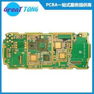
Supplier: Shenzhen Grande Electronic Layers: 4 Application: Welding Machine Immersion Gold PCB Prototype / PCB Manufacturer China PCB Parameter: FR-4/HTG150 Thickness:1.6mm Surface Treatment: Immersion Gold Testing: 100% E-test Package: Vacuum packi

New Equipment | Board Handling - Storage
Supplier: Grande Electronics Layers: 4 Application: Pager Electronic Manufacturing | Fusion PCB Fabrication & Prototype PCB Parameter: FR-4/HTG150 Thickness: 1.6mm Surface Treatment: ENIG Testing: 100% E-test Package: Vacuum packing Lead Time: 10-15
New Equipment | Board Handling - Pallets,Carriers,Fixtures
Supplier: Grande Layers: 4 Application: Asset Tracking Device and System Turnkey PCB Solution - Printed Circuit Board Manufacturer PCB Parameter: FR-4/HTG150 Thickness: 1.6mm Surface Treatment: HASL Testing: 100% E-test Package: Vacuum packing Lead


