New Equipment | Cleaning Equipment
The Gensonic Stencil Cleaning System, awarded the European Product of the Year at Productronica 2013, is a manually operated ultrasonic transducer unit for cleaning stencil apertures. The Gensonic can be used either in conjunction with our Stencil Cl
Industry News | 2012-12-03 16:09:15.0
LPKF Laser & Electronics will present the webinar Stencil Aperture Size and Its Impact on the Printing Process Thursday, December 6, 2012 at 11 a.m. PST. The webinar examines the relationship between stencil aperture size and solder paste volume and how the stencil manufacturing process can influence both.
Technical Library | 2017-09-28 16:36:33.0
These nano-coatings also refine the solder paste brick shape giving improved print definition. These two benefits combine to help the solder paste printing process produce an adequate amount of solder paste in the correct position on the circuit board pads. Today, stencil aperture area ratios from 0.66 down to 0.40 are commonly used and make paste printing a challenge. This paper presents data on small area ratio printing for component designs including 01005 Imperial (0402 metric) and smaller 03015 metric and 0201 metric chip components and 0.3 mm and 0.4 mm pitch micro BGAs.
Technical Library | 2012-10-25 16:34:02.0
First published in the 2012 IPC APEX EXPO technical conference proceedings. This paper will examine stencil technologies (including Laser and Electroform), Aperture Wall coatings (including Nickel-Teflon coatings and Nano-coatings), and how these parameters influence paste transfer for miniature devices with Area Ratios less than the standard recommended lower limit of .5. A matrix of print tests will be utilized to compare paste transfer and measure the effectiveness of the different stencil configurations. Area Ratios ranging from .32 to .68 will be investigated.

New Equipment | Solder Paste Stencils
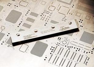
Stentech has its very own high quality stencil rolls, designed for use in SMT (Surface Mount Technology) and screen printing lines. These rolls are designed to keep stencil apertures clear of paste residues during the automatic screen printing proces
.JPG)
Used SMT Equipment | SPI / Solder Paste Inspection
The LSM300 follows the successful Laser section Microscopes LSM and LSM2. This new non-contact laser based system is an off-Line solder paste inspection system.LSM300 provides automatic height measurements, eliminating the inconsistencies of manual m
Technical Library | 2023-07-25 16:25:56.0
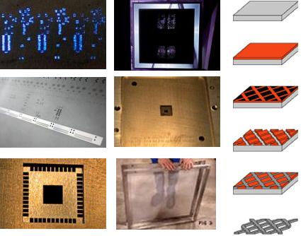
This paper address two significant applications of stencils in advance packaging field: 1. Ultra-Thin stencils for miniature component (0201m) assembly; 2. Deep Cavity stencils for embedded (open cavity) packaging. As the world of electronics continues to evolve with focus on smaller, lighter, faster, and feature-enhanced high- performing electronic products, so are the requirement for complex stencils to assemble such components. These stencil thicknesses start from less than 25um with apertures as small as 60um (or less). Step stencils are used when varying stencil thicknesses are required to print into cavities or on elevated surfaces or to provide relief for certain features on a board. In the early days of SMT assembly, step stencils were used to reduce the stencil thickness for 25 mil pitch leaded device apertures. Thick metal stencils that have both relief-etch pockets and reservoir step pockets are very useful for paste reservoir printing. Electroform Step-Up Stencils for ceramic BGA's and RF Shields are a good solution to achieve additional solder paste height on the pads of these components as well as providing exceptional paste transfer for smaller components like uBGAs and 0201s. As the components are getting smaller, for example 0201m, or as the available real estate for component placement on a board is getting smaller – finer is the aperture size and the pitch on the stencils. Aggressive distances from step wall to aperture are also required. Ultra-thin stencils with thicknesses in the order of 15um-40um with steps of 15um are used to obtain desired print volumes. Stencils with thickness to this order can be potential tools even to print for RDLs in the package.
New Equipment | Assembly Services
Fine Line Stencil is Committed to Delivering the Highest Quality Laser Stencils in the Industry LPKF Laser Technology / SMT Stencil Laser Technology Laser Slic Stencils / Laser Ultra Slic Stencils Custom Apertures Dog Bone, Home Plate, K
Industry Directory | Manufacturer
Manufacturer of Laser Cut & Chemical Etched Stencils.
New Equipment | Solder Paste Stencils
Laser Cut Stencils: Industry trend toward miniaturization is leading to finer pitch requirements, high tolerances, and greater repeatability. Our state-of-the-art laser technology enables our customers to experience positional accuracy unattainable w


.jpg)
