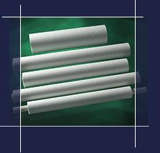
New Equipment | Solder Paste Stencils
EasyBraid’s stencil rolls are designed for use in SMT screen printing lines which keep stencil apertures clear of paste residues during the automatic screen printing process. They also clean the bottom of stencils, keeping them free from paste and fl
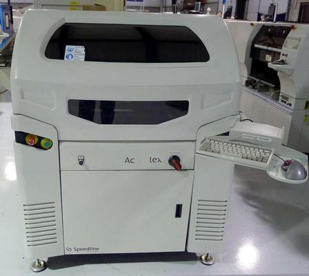
Used SMT Equipment | Screen Printers
Grid-Lok Tooling is the most flexible PCB support on the SMT market, for the entire assembly process. This unique concept combines the benefits of manual locking modules with the extensive advantages of automatic tooling systems. Easy upgradeability
?????VOC????????????????????? =??= http://www.sawa-corp.co.jp/product/sc_ah100

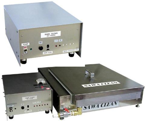
The Sawa Eco-Roll eliminates waste and saves money by reusing wiper rolls for printing machines. The SC-ER360 cleans wiper rolls in just 20 minutes and measures W900 x D850 x H1200 mm. Sawa Stencil Cleaners are widely used in the Japanese electronic
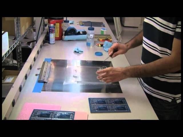
This is video shows how to print a PCB using a prototype foil only stencil. The SMT prototype stencil (www.soldertools.net) is made from a high nickel content material able to offer repeatable high precision apertures. The steps of alignment, printin
Industry News | 2001-08-02 12:48:27.0
Inspect stencils & screens for accuracy, cleanliness, damage, distortion and create Gerber data.
New Equipment | Cleaning Equipment
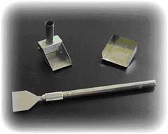
Precision Fine Pitch Aperture Cleaners Thousands of dollars less than fully-automatic cleaners Low solvent usage and running costs Fast cleaning time of 1-3 minutes Minimal waste disposal Portable unit can be used directly on the screen printe
The G-Titan printer offers Opti-Paste Control (OPC), get ready for lights-out manufacturing! Quality Print Control (QPC) Solder Paste Rolling Measurement Stencil Lock Automatic Solder Paste Dispense FEATURES: Auto Paste Dispensing - Paste
New Equipment | Solder Paste Stencils
Stentech produces mini stencils; small stencils that are used mainly for BGA re-work. Mini stencils are designed to deposit precise amounts of solder paste for single BGA footprints on loaded PCBs. These precision stencils mimic the footprint and ape
Technical Library | 2018-09-26 20:33:26.0
Bottom terminated components, or BTCs, have been rapidly incorporated into PCB designs because of their low cost, small footprint and overall reliability. The combination of leadless terminations with underside ground/thermal pads have presented a multitude of challenges to PCB assemblers, including tilting, poor solder fillet formation, difficult inspection and – most notably – center pad voiding. Voids in large SMT solder joints can be difficult to predict and control due to the variety of input variables that can influence their formation. Solder paste chemistries, PCB final finishes, and reflow profiles and atmospheres have all been scrutinized, and their effects well documented. Additionally, many of the published center pad voiding studies have focused on optimizing center pad footprint and stencil aperture designs. This study focuses on I/O pad stencil modifications rather than center pad modifications. It shows a no-cost, easily implemented I/O design guideline that can be deployed to consistently and repeatedly reduce void formation on BTC-style packages.


.png)
