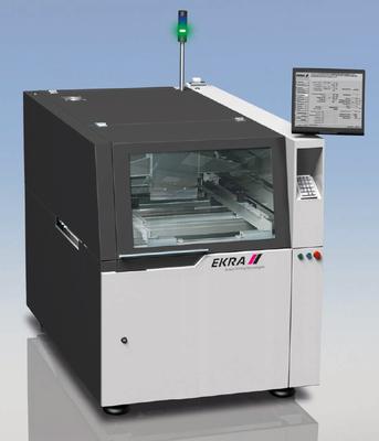
The XACT 4 automatic screen and stencil printer is specially designed to perform any kind of production demands within the electronic industry, and therefore paying special attention to its universal usage. The XACT 4 features the exceptional EKRA ea
Industry News | 2018-10-18 10:24:05.0
The Design Principles of Stencil Apertures
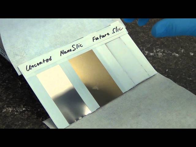
NanoSlic™ Gold is our top of the line spray on coating applied to our UltraSlic™ solder paste stencil, which gives previously unseen performance benefits in transfer efficiency. The NanoSlic™ Gold coating also gives the benefits of improved under-ste
New Equipment | Solder Paste Stencils
PNC Inc. uses LPKF Laser Technology to manufacture SMT Solder paste stencil, high tolerance aperture openings with superior registration for it’s solder paste stencils. With it’s 4 mil beam diameter, our Laser is capable of cutting small aperture ope
Technical Library | 2014-06-05 16:44:07.0
Stencil printing capability is becoming more important as the range of component sizes assembled on a single board increases. Coupled with increased component density, solder paste sticking to the aperture sidewalls and bottom of the stencil can cause insufficient solder paste deposits and solder bridging. Yield improvement requires increased focus on stencil technology, printer capability, solder paste functionality and understencil cleaning.(...) The purpose of this research is to study the wipe sequence, wipe frequency and wipe solvent(s) and how these factors interact to provide solder paste printing yield improvement.
Industry Directory | Manufacturer
Manufacturer of Laser cut stencils, thick film screens, large format screens. Variety of stainless steel materials and mesh, ITAR registered. Member of SMTA, IMAPS and IPC.

ALPHA® TETRABOND™ is the culmination of "frameless" stencil development; an elegantly simple system designed to enhance the rigidity of the foil, making safe mounting and demounting an easier proposition. Innovatively encompassed in a thin, one piece
New Equipment | ESD Control Supplies
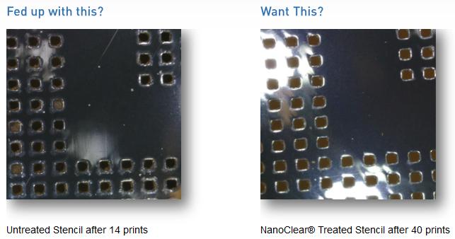
High performance fluxophobic stencil treatments wipes Enhance your stencil performance in seconds! Aculon is pleased to announce the launch of their latest generation of stencil coating technology. Aculon’s proprietary technology treats the undersi
Technical Library | 2023-07-25 16:50:02.0
Some of the new handheld communication devices offer real challenges to the paste printing process. Normally, there are very small devices like 01005 chip components as well as 0.3 mm pitch uBGA along with other devices that require higher deposits of solder paste. Surface mount connectors or RF shields with coplanarity issues fall into this category. Aperture sizes for the small devices require a stencil thickness in the 50 to 75 um (2-3 mils) range for effective paste transfer whereas the RF shield and SMT connector would like at least 150 um (6 mils) paste height. Spacing is too small to use normal step stencils. This paper will explore a different type of step stencil for this application; a "Two-Print Stencil Process" step stencil. Here is a brief description of a "Two-Print Stencil Process". A 50 to 75 um (2-3 mils) stencil is used to print solder paste for the 01005, 0.3 mm pitch uBGA and other fine pitch components. While this paste is still wet a second in-line stencil printer is used to print all other components using a second thicker stencil. This second stencil has relief pockets on the contact side of the stencil any paste was printed with the first stencil. Design guidelines for minimum keep-out distances between the relief step, the fine pitch apertures, and the RF Shields apertures as well relief pocket height clearance of the paste printed by the first print stencil will be provided.
Industry News | 2012-04-09 13:45:59.0
As the electronics assembly industry evolves, printed circuit board (PCB) features and surface mount technology (SMT) components continue to get smaller and smaller. This miniaturization shrinks the process window at print, placement, and reflow, increasing the opportunities for defects.


