New Equipment | Fabrication Services
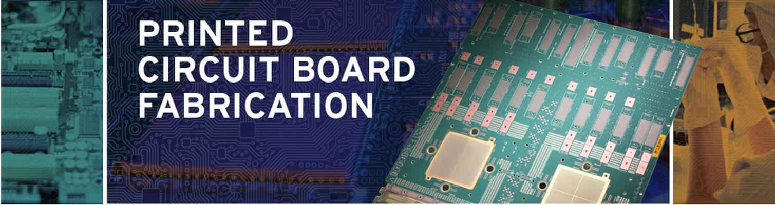
High Layer Count, High Complexity, High Reliability. At i3 Electronics, we offer the total package for your printed circuit board fabrication. We can design, manufacture, assemble, and test your PCB. Our specialty is high layer count, high complexi

Industry News | 2011-02-07 15:33:41.0
Multitest announces that Chris Cuda, US Product Manager, will present a paper titled "Benefits & Risks of High Aspect Ratio Vias in ATE Boards" at the upcoming Burn-in & Test Socket Workshop, scheduled to take place March 6-9, 2011 at the Hilton Phoenix East/Mesa Hotel in Mesa, Arizona.
Industry News | 2011-10-12 21:39:45.0
Multitest announces that the Santa Clara board fab has refined its pulse plating process to integrate it into Multitest’s fabrication process to further enhance the high aspect ratio capability.
Technical Library | 2019-07-17 17:56:34.0
The increased demand for electronic devices in recent years has led to an extensive research in the field to meet the requirements of the industry. Electrolytic copper has been an important technology in the fabrication of PCBs and semiconductors. Aqueous sulfuric acid baths are explored for filling or building up with copper structures like blind micro vias (BMV), trenches, through holes (TH), and pillar bumps. As circuit miniaturization continues, developing a process that simultaneously fills vias and plates TH with various sizes and aspect ratios, while minimizing the surface copper thickness is critical. Filling BMV and plating TH at the same time, presents great difficulties for the PCB manufactures. The conventional copper plating processes that provide good via fill and leveling of the deposit tend to worsen the throwing power (TP) of the electroplating bath. TP is defined as the ratio of the deposit copper thickness in the center of the through hole to its thickness at the surface. In this paper an optimization of recently developed innovative, one step acid copper plating technology for filling vias with a minimal surface thickness and plating through holes is presented.
Industry Directory | Manufacturer
Founded in 1992, LaserJob specializes in laser-cut stencils for printed circuit boards used in electronic devices.

Innovative Materials, Superior Performance. Our printed circuit board and semiconductor packaging materials provide superior thermal and mechanical performance, a fact we’ve prided ourselves on for over 45 years. All our materials are RoHS complian

New Equipment | Assembly Services
Quick turn Prototype PCBs from 24 hour turnaround to high volume printed circuit board production from our domestic plant in USA and/or China facilities. Our Modern 38,000 sq. ft. manufacturing plant with multi-million dollar investment with latest e
Technical Library | 2022-08-08 15:06:06.0
Selective soldering has evolved to become a standard production process within the electronics assembly industry, and now accommodates a wide variety of through-hole component formats in numerous applications. Most through-hole components can be easily soldered with the selective soldering process without difficulty however some types of challenging components require additional attention to ensure that optimum quality is maintained. Several high thermal mass components can place demands on the selective soldering process, while the use of specialized solder fixtures, or solder pallets, often places additional thermal demand on the preheating process. Fine-pitch through-hole components and connectors place a different set of demands on the selective soldering process and typically require special attention to lead projection and traverse speed to minimize bridging between adjacent pins. Dual in-line memory module (DIMM) connectors, compact peripheral component interface (cPCI) connectors, coax connectors and other high thermal mass components as well as fine-pitch microconnectors, can present challenges when soldered into backplanes or multilayer printed circuit board assemblies. Adding to this challenge, compact peripheral component interface connectors can present additional solderability issues because of their beryllium copper base metal pins. Key Terms: Selective soldering, drop-jet fluxing, sustained preheating, flux migration, adjacent clearance, lead-to-hole aspect ratio, lead projection, thermal reliefs, gold embrittlement, solderability testing.
Industry News | 2003-03-11 09:04:04.0
Developed in response to customer requirements, the new Via Fill process from DEK delivers 100% fill of substrate vias with no voids and minimal surface residue.


