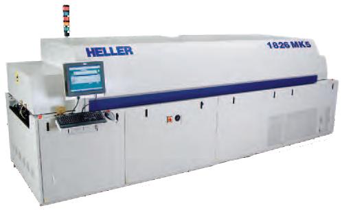
The World's Best SMT Convection Reflow Ovens for Large Boards and Dual Lane 1826 Mark 5 reflow oven provides consistent performance for high volume reflow requirements while minimizing preventative maintenance and floorspace. Lead Free Certified!
Used SMT Equipment | Soldering - Reflow
10 Heat Zones Voltage: 380V Max PCB size: 18" Feed Direction: L-R Additional Options: EHC, Dual Lane (MFFM), Fan Speed Control, CBS, Reactor, Cool Pipe
Nano-copper sintering in formic acid vapor.
Technical Library | 2020-01-28 00:23:58.0
This paper explores new advances in the reflow soldering process including vacuum technology and warpage mitigation systems. The first topic for discussion will be the implementation of a vacuum process directly in a conventional inline soldering system. The second topic presented is the mitigation of warpage on substrates or wafers.
Technical Library | 2023-01-17 18:07:31.0
To achieve higher levels of consistency in PCB output, process engineers are able to maintain tighter controls and reduce process-related defects by using closed-loop process controls. At every stage of assembly, from screen printing through placement to reflow, closed-loop systems help control the variable factors that can have adverse effects on the process.
Technical Library | 2023-01-17 17:27:13.0
Reflow profile has significant impact on solder joint performance because it influences wetting and microstructure of the solder joint. The degree of wetting, the microstructure (in particular the intermetallic layer), and the inherent strength of the solder all factor into the reliability of the solder joint. This paper presents experimental results on the effect of reflow profile on both 63%Sn 37%Pb (SnPb) and 96.5%Sn 3.0%Ag 0.5%Cu (SAC 305) solder joint shear force. Specifically, the effect of the reflow peak temperature and time above solder liquidus temperature are studied. Nine reflow profiles for SAC 305 and nine reflow profiles for SnPb have been developed with three levels of peak temperature (230 o C, 240 o C, and 250 o C for SAC 305; and 195 o C, 205 o C, and 215 o C for SnPb) and three levels of time above solder liquidus temperature (30 sec., 60 sec., and 90 sec.). The shear force data of four different sizes of chip resistors (1206, 0805, 0603, and 0402) are compared across the different profiles. The shear force of the resistors is measured at time 0 (right after assembly). The fracture surfaces have been studied using a scanning electron microscopy (SEM) with energy dispersive spectroscopy (EDS)
Technical Library | 2023-01-17 18:04:51.0
As a manufacturing technology, SMT has acquired a "heritage" of widely accepted assumptions about its processes. However, yesterday'spractices are continually confronted by the shifting paradigms of today's production line.
Events Calendar | Wed Oct 02 00:00:00 EDT 2019 - Thu Oct 03 00:00:00 EDT 2019 | Fremont, California USA
i4.0 Connect Forum
Technical Library | 2023-01-17 17:12:33.0
Reflowed indium metal has for decades been the standard for solder thermal interface materials (solder TIMs or sTIMs) in most high-performance computing (HPC) TIM1 applications. The IEEE Heterogeneous Integration Thermal roadmap states that new thermal interface materials solutions must provide a path to the successful application of increased total-package die areas up to 100cm2. While GPU architectures are relatively isothermal during usage, CPU hotspots in complex heterogeneously-integrated modules will need to be able to handle heat flux hotspots up to 1000W/cm2 within the next two years. Indium and its alloys are used as reflowed solder thermal interface materials in both CPU and GPU "die to lid/heat spreader" (TIM1) applications. Their high bulk thermal conductivity and proven long-term reliability suit them well for extreme thermomechanical stresses. Voiding is the most important failure mode and has been studied by x-ray. The effects of surface pretreatment, pressure during reflow, solder flux type/fluxless processing, and preform design parameters, such as alloy type, are also examined. The paper includes data on both vacuum and pressure (autoclave) reflow of sTIMs, which is becoming necessary to meet upcoming requirements for ultralow voiding in some instances.
Technical Library | 2023-01-17 17:58:36.0
Heterogeneous integration has become an important performance enabler as high-performance computing (HPC) demands continue to rise. The focus to enable heterogeneous integration scaling is to push interconnect density limit with increased bandwidth and improved power efficiency. Many different advanced packaging architectures have been deployed to increase I/O wire / area density for higher data bandwidth requirements, and to enable more effective die disaggregation. Embedded Multi-die Interconnect Bridge (EMIB) technology is an advanced, cost-effective approach to in-package high density interconnect of heterogeneous chips, providing high density I/O, and controlled electrical interconnect paths between multiple dice in a package. In emerging architectures, it is required to scale down the EMIB die bump pitch in order to further increase the die-to-die (D2D) communication bandwidth. Aa a result, bump pitch scaling poses significant challenges in the plated solder bump reflow process, e.g., bump height / coplanarity control, solder wicking control, and bump void control. It's crucial to ensure a high-quality solder bump reflow process to meet the final product reliability requirements. In this paper, a combined formic acid based fluxless and vacuum assisted reflow process is developed for fine pitch plated solder bumping application. A high-volume production (HVM) ready tool has been developed for this process.


winsouce.jpg)