Industry Directory | Manufacturer
Micralyne offers a patented process for electroplating AuSn solder alloy, at compositions from 10 to 40 Sn (wt%), in patterned or unpatterned shapes onto metallized substrates at virtually any thickness.
Industry Directory | Manufacturer
We are manufacturer of key products for semiconductor back end process and interconnect materials. Our main products:solder balls, Bonding wire (Au, Ag, Cu, Pd-Cu),sputtering target & EVM materials.
New Equipment | Soldering - Other
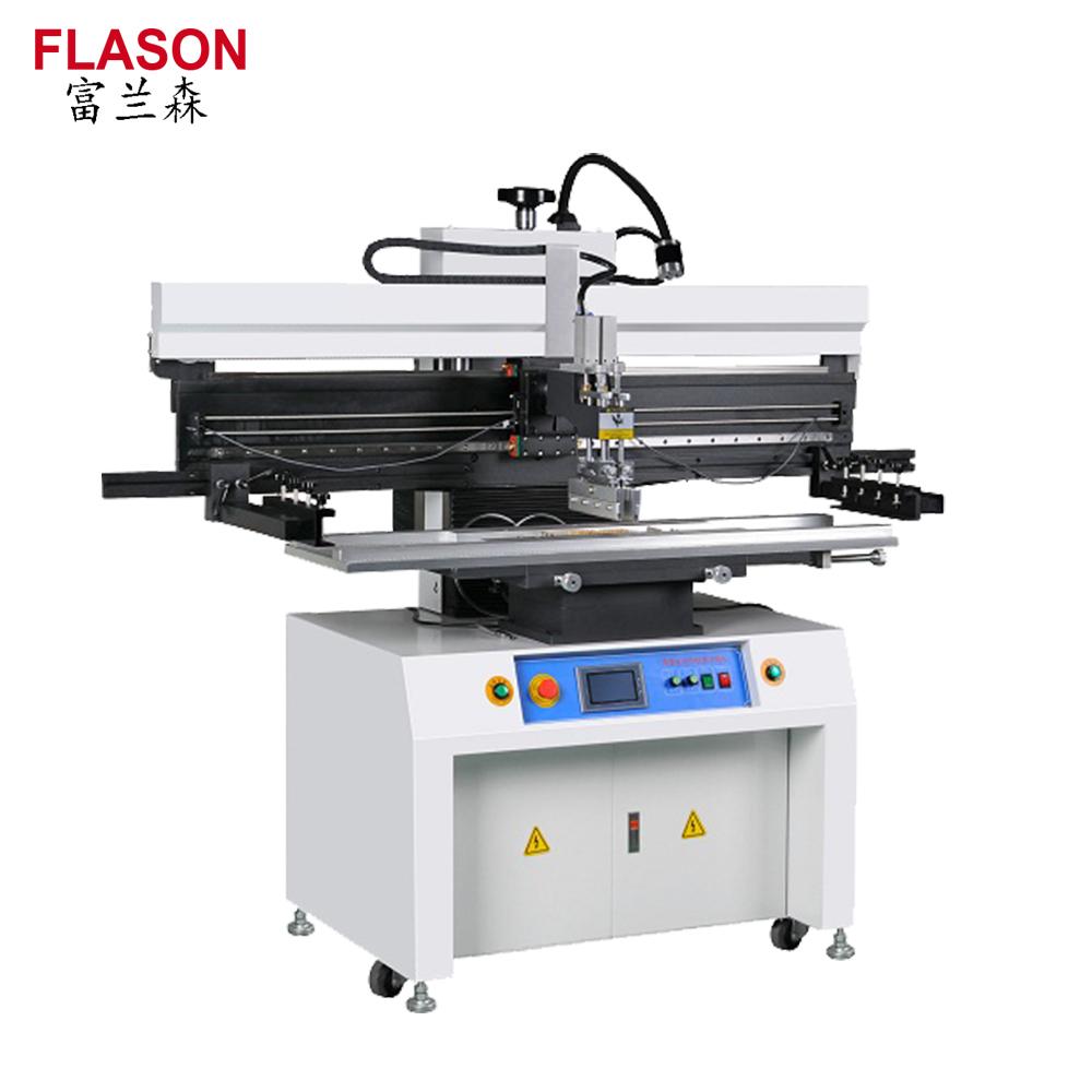
SMT Stencil Printer Touch screen Manual stencil printing machine / solder paste printer pcb size: 1200mm*390mm Weight: 310KG Dimensions(L*W*H): 880*780*1630MM Voltage: 220V/50-60HZ Product description: Touch screen Manual ste
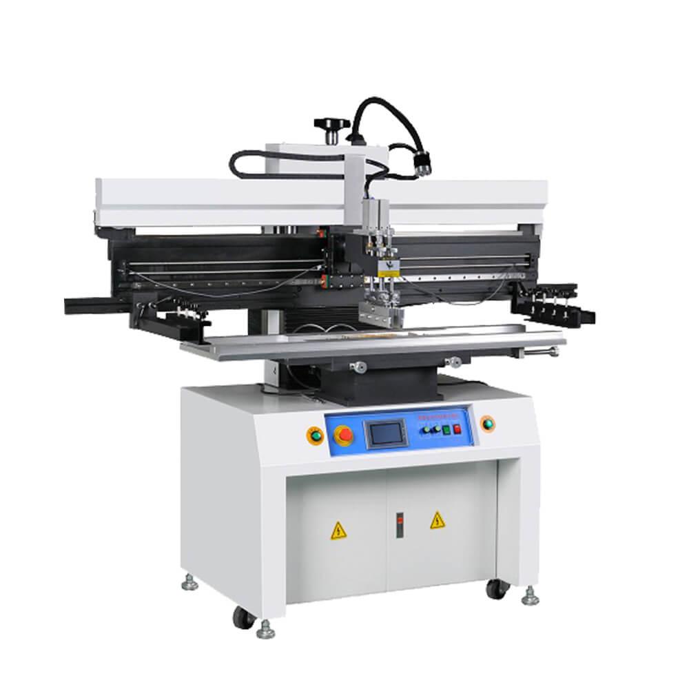
Flason SMT China SMT stencil printer factory Manufacturer pcb size: 1200mm*390mm Weight: 310KG Dimensions(L*W*H): 880*780*1630MM Voltage: 220V/50-60HZ Product description: China SMT stencil printer factory Manufacturer-Good Price! Good Qualit
Industry News | 2003-03-11 08:45:00.0
CAMtastic DXP is the latest version of Altium's complete CAM verification and editing system that bridges the gap between PCB design and manufacturing and facilitates communication between board designers, fabrication engineers, and their clients.
Industry News | 2013-08-01 13:16:42.0
The SMTA announced that the Lead-Free Soldering Technology Symposium will be held on October 17, 2013 as a focused symposium at SMTA International in Fort Worth, TX.
Technical Library | 2013-08-29 19:52:43.0
Au over Ni on Cu is a widely used printed circuit board (PCB) surface finish, under bump metallization (UBM), and component lead metallization. It is generally accepted that less than 3 wt.% Au in Sn-Pb solder joints inhibits formation of detrimental intermetallic compounds (IMC). However, the critical limit for Au content in Pb-free solder joints is not well established. Three surface-mount package platforms, one with a matte Sn surface finish and the others with Ni/Au finish, were soldered to Ni/Au-finished PCB using Sn-3.0Ag 0.5Cu (SAC305) solder, in a realistic manufacturing setting. The assembled boards were divided into three groups: one without any thermal treatment, one subjected to isothermal aging at 125°C for 30 days, and the third group aged at 125°C for 56 days...
Technical Library | 2012-10-18 21:58:51.0
First published in the 2012 IPC APEX EXPO technical conference proceedings. In this paper, we report on a comprehensive study regarding the morphology evolution and voiding of SnAgCu solder joints on the central pad of two different packages – QFN and an Agilent package called TOPS – on PCBs with a Ni/Au surface finish.
The FINEPLACER® Lambda, a modularly designed bonder, provides a full range of process capabilities and multiple bonding technologies. Read more: http://eu.finetech.de/micro-assembly/products/fineplacerr-lambda.html

Inline 3D SPI, Standard Automatic solder paste inspection system As one of the strongest SMT 3D SPI Manufacuturer in China, we provide you all the different models of online solder paste inspection machine,we have variety of size and models of the
Career Center | St. Léonard, Quebec Canada | Production
Joignez-vous à Schneider Electric et propulsez votre carrière! Découvrez l’occasion rêvée de vous joindre à une entreprise internationale, dynamique et responsable qui encourage le développement de tous ses employés à travers le monde. Chaque jour,
Career Center | Flower Mound, Texas USA | Engineering,Management,Production,Quality Control,Research and Development,Technical Support
SMT and THT Soldering Process Optimization Working knowledge of MPM Screen Printers, Fuji and Siemens Placement Equipment, BTU, ERSA and Vitronics Reflow Ovens, Camalot 3500 Underfill Dispense Machine, SEHO and Electrovert Wave Soldering Systems
Career Center | , | Engineering,Production,Quality Control,Research and Development
WORK EXPERIENCE Hutchinson Technology Incorporated, MN Feb.2006-Present Process Development Engineering Co-op �Study of voids generation in solder ball bonded Cu substrate with Ni/Au metallization. �Diffusion & Intermetallic growth study in sold
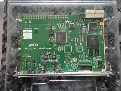
The Morphology Evolution and Voiding of Solder Joints on QFN Central Pads with a Ni/Au Finish SMTnet Express October 19, 2012, Subscribers: 25598, Members: Companies: 9011, Users: 33828 The Morphology Evolution and Voiding of Solder Joints on QFN
SMTnet Express August 29, 2013, Subscribers: 26233, Members: Companies: 13474, Users: 35110 Effect of Gold Content on the Microstructural Evolution of SAC305 Solder Joints Under Isothermal Aging by Mike Powers, Jianbiao Pan, Julie Silk, Patrick
| https://www.eptac.com/wp-content/uploads/2007/10/webinar_eptac_10_17_07.pdf
Heller Industries Inc. | https://hellerindustries.com/wp-content/uploads/2022/06/Optimizing-Reflowed-Solder-TIM-sTIMs-Processes-for-Emerging-Heterogeneous.pdf
to be joined using sTIM are usually gold, with the silicon backside typically being PVD-deposited Ti/NiV/Au (80-200nm Au), and copper heatspreader/lids plated with Ni/Au (usually with 0.3-0.8um Au). Except for the inevitable presence of a film of