Technical Library | 2022-06-27 16:50:26.0
Electronics industry is one of the fastest evolving, innovative, and most competitive industries. In order to meet the high consumption demands on electronics components, quality standards of the products must be well-maintained. Automatic optical inspection (AOI) is one of the non-destructive techniques used in quality inspection of various products. This technique is considered robust and can replace human inspectors who are subjected to dull and fatigue in performing inspection tasks. A fully automated optical inspection system consists of hardware and software setups. Hardware setup include image sensor and illumination settings and is responsible to acquire the digital image, while the software part implements an inspection algorithm to extract the features of the acquired images and classify them into defected and non-defected based on the user requirements. A sorting mechanism can be used to separate the defective products from the good ones. This article provides a comprehensive review of the various AOI systems used in electronics, micro-electronics, and opto-electronics industries. In this review the defects of the commonly inspected electronic components, such as semiconductor wafers, flat panel displays, printed circuit boards and light emitting diodes, are first explained. Hardware setups used in acquiring images are then discussed in terms of the camera and lighting source selection and configuration. The inspection algorithms used for detecting the defects in the electronic components are discussed in terms of the preprocessing, feature extraction and classification tools used for this purpose. Recent articles that used deep learning algorithms are also reviewed. The article concludes by highlighting the current trends and possible future research directions.
Industry News | 2009-07-24 13:20:42.0
San Diego — July 2009 — KIC announces the release of the e-Clipse, a solar cell thermocouple (TC) attachment fixture.

Flip Chip Thermosonic Bonding with the FINEPLACER® pico MA. http://eu.finetech.de/micro-assembly/products/fineplacerr-pico-ma.html More information about Thermosonic bonding: http://eu.finetech.de/micro-assembly/technologies/ultrasonic-thermosonic-b
Industry News | 2014-11-03 19:19:11.0
The Fastest Fully Automatic X-ray Metrology tool for Wafer Bumps and TSV’s.
Industry News | 2007-11-15 19:16:35.0
Medway, MA � November 15, 2007 � Milara Inc., a leading vendor of fully and semiautomatic stencil printers for SMT and semiconductor applications, announces that it has been awarded a Global Technology Award in the category of Wafer-level Products for its innovative AWPb 300.
Industry News | 2013-06-20 19:12:14.0
Tresky, announces that it will display the T-6000 Flexible Automatic Die Bonder in Booth #5770 at the 2013 SEMICON West exhibition & conference, scheduled to take place July 9-11, 2013 at the Moscone Center in San Francisco, CA. Tresky will co-exhibit with XYZTEC.

New Equipment | Test Equipment
Xynetics 1034X Die Prober Test Station with Olympus Microscope head. The eye pieces are Olympus G20x 12.2. We are unable to test this prober. Cables for the controller to connect to the probe station are not available. Contact for freight shipping de
Industry News | 2011-08-03 21:32:16.0
Cognex Corporation has introduced its next-generation wafer identification (ID) reader and accompanying software, the In-Sight® 1740 series and In-Sight Explorer Wafer ID software version 4.5.0.
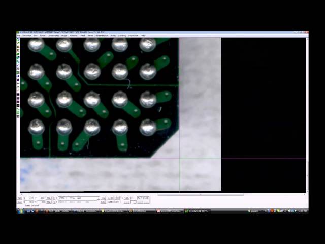
ScanCOMPONENT is a PC-based offline component programming system for the creation of vision data files from the smallest flip chip and bumped packages to the largest odd form devices. The ScanCOMPONENT is a standalone Product as well as a module of
The Microelectronics Lab was established to meet the rising need for advanced systems development and packaging to address the emerging challenges and issues facing today’s electronics assemblies. Advanced design and modeling software enables STI to


