Industry News | 2013-02-20 18:54:10.0
IPC — Association Connecting Electronics Industries® presented Committee Leadership, Distinguished Committee Service and Special Recognition Awards at IPC APEX EXPO® at the San Diego Convention Center.
Industry News | 2019-11-05 22:19:03.0
> News-Blog > Guideline for wire bonding Guideline for wire bonding Tuesday,Jun 12,2018 There are two wire bonding processes that are used, Thermosonic (T/S) Gold Ball Wire Bonding and Ultrasonic (U/S) Aluminum Wedge Wire Bonding. Approximately 90% of all IC Assembly in Semiconductor Packages is manufactured using Gold Ball Bonding process, while Aluminum Wedge Bonding is used to produce about 10% of other Wire Bonding requirements on Printed Circuit Boards (PCB), Printed Circuit Flex (PCF) and other Packages.
Industry Directory | Manufacturer
We are manufacturer of key products for semiconductor back end process and interconnect materials. Our main products:solder balls, Bonding wire (Au, Ag, Cu, Pd-Cu),sputtering target & EVM materials.
Career Center | Philadelphia, New Jersey USA | Sales/Marketing
LOCATION BASE SALARY USA - NJ - Central USA - NJ - Southern USA - PA - Philadelphia $67000 - 73000 Another $50K to $70K in commissions based on plan COMPANY BRIEF My client is a leading supplier of automated broadband communications assembly e
Technical Library | 2017-09-07 13:56:11.0
As a surface finish for PCBs, Electroless Nickel/Electroless Palladium/Immersion Gold (ENEPIG) was selected over Electroless Nickel/Immersion Gold (ENIG) for CMOS image sensor applications with both surface mount technology (SMT) and gold ball bonding processes in mind based on the research available on-line. Challenges in the wire bonding process on ENEPIG with regards to bondability and other plating related issues are summarized.
Used SMT Equipment | Semiconductor & Solar
Standard Machine features and system description: Ultra-fine pitch and small ball bonding capabilities High frequency transducer operating at 138 kHz Applicable wire size of 0.6mil-2.0mil High speed XY table with linear motor technology High ac
High Speed, Large Area (12in x 6in.) Ball bonder with Continuous Bonding Technology.
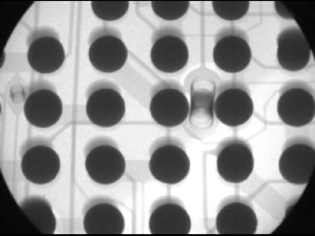
Technical Library | 2020-08-27 01:22:45.0
Initially adopted internal specifications for acceptance of printed circuit boards (PCBs) used for wire bonding was that there were no nodules or scratches allowed on the wirebond pads when inspected under 20X magnification. The nodules and scratches were not defined by measurable dimensions and were considered to be unacceptable if there was any sign of a visual blemish on wire-bondable features. Analysis of the yield at a PCB manufacturer monitored monthly for over two years indicated that the target yield could not be achieved, and the main reasons for yield loss were due to nodules and scratches on the wirebonding pads. The PCB manufacturer attempted to eliminate nodules and scratches. First, a light-scrubbing step was added after electroless copper plating to remove any co-deposited fine particles that acted as a seed for nodules at the time of copper plating. Then, the electrolytic copper plating tank was emptied, fully cleaned, and filtered to eliminate the possibility of co-deposited particles in the electroplating process. Both actions greatly reduced the density of the nodules but did not fully eliminate them. Even though there was only one nodule on any wire-bonding pad, the board was still considered a reject. To reduce scratches on wirebonding pads, the PCB manufacturer utilized foam trays after routing the boards so that they did not make direct contact with other boards. This action significantly reduced the scratches on wire-bonding pads, even though some isolated scratches still appeared from time to time, which caused the boards to be rejected. Even with these significant improvements, the target yield remained unachievable. Another approach was then taken to consider if wire bonding could be successfully performed over nodules and scratches and if there was a dimensional threshold where wire bonding could be successful. A gold ball bonding process called either stand-off-stitch bonding (SSB) or ball-stitch-on-ball bonding (BSOB) was used to determine the effects of nodules and scratches on wire bonds. The dimension of nodules, including height, and the size of scratches, including width, were measured before wire bonding. Wire bonding was then performed directly on various sizes of nodules and scratches on the bonding pad, and the evaluation of wire bonds was conducted using wire pull tests before and after reliability testing. Based on the results of the wire-bonding evaluation, the internal specification for nodules and scratches for wirebondable PCBs was modified to allow nodules and scratches with a certain height and a width limitation compared to initially adopted internal specifications of no nodules and no scratches. Such an approach resulted in improved yield at the PCB manufacturer.


