High Speed, Large Area (12in x 6in.) Ball bonder with Continuous Bonding Technology.
Technical Library | 2020-08-27 01:22:45.0
Initially adopted internal specifications for acceptance of printed circuit boards (PCBs) used for wire bonding was that there were no nodules or scratches allowed on the wirebond pads when inspected under 20X magnification. The nodules and scratches were not defined by measurable dimensions and were considered to be unacceptable if there was any sign of a visual blemish on wire-bondable features. Analysis of the yield at a PCB manufacturer monitored monthly for over two years indicated that the target yield could not be achieved, and the main reasons for yield loss were due to nodules and scratches on the wirebonding pads. The PCB manufacturer attempted to eliminate nodules and scratches. First, a light-scrubbing step was added after electroless copper plating to remove any co-deposited fine particles that acted as a seed for nodules at the time of copper plating. Then, the electrolytic copper plating tank was emptied, fully cleaned, and filtered to eliminate the possibility of co-deposited particles in the electroplating process. Both actions greatly reduced the density of the nodules but did not fully eliminate them. Even though there was only one nodule on any wire-bonding pad, the board was still considered a reject. To reduce scratches on wirebonding pads, the PCB manufacturer utilized foam trays after routing the boards so that they did not make direct contact with other boards. This action significantly reduced the scratches on wire-bonding pads, even though some isolated scratches still appeared from time to time, which caused the boards to be rejected. Even with these significant improvements, the target yield remained unachievable. Another approach was then taken to consider if wire bonding could be successfully performed over nodules and scratches and if there was a dimensional threshold where wire bonding could be successful. A gold ball bonding process called either stand-off-stitch bonding (SSB) or ball-stitch-on-ball bonding (BSOB) was used to determine the effects of nodules and scratches on wire bonds. The dimension of nodules, including height, and the size of scratches, including width, were measured before wire bonding. Wire bonding was then performed directly on various sizes of nodules and scratches on the bonding pad, and the evaluation of wire bonds was conducted using wire pull tests before and after reliability testing. Based on the results of the wire-bonding evaluation, the internal specification for nodules and scratches for wirebondable PCBs was modified to allow nodules and scratches with a certain height and a width limitation compared to initially adopted internal specifications of no nodules and no scratches. Such an approach resulted in improved yield at the PCB manufacturer.
Technical Library | 2014-07-24 16:26:34.0
Wire bonding a die to a package has traditionally been performed using either aluminum or gold wire. Gold wire provides the ability to use a ball and stitch process. This technique provides more control over loop height and bond placement. The drawback has been the increasing cost of the gold wire. Lower cost Al wire has been used for wedge-wedge bonds but these are not as versatile for complex package assembly. The use of copper wire for ball-stitch bonding has been proposed and recently implemented in high volume to solve the cost issues with gold. As one would expect, bonding with copper is not as forgiving as with gold mainly due to oxide growth and hardness differences. This paper will examine the common failure mechanisms that one might experience when implementing this new technology.
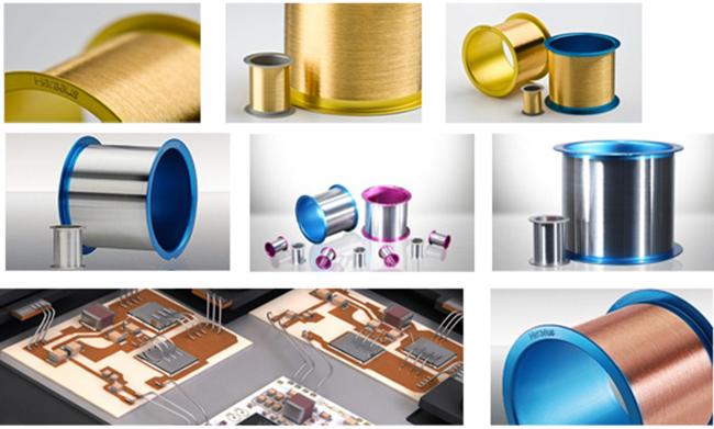
Gold / Aluminum / Copper Bonding Wires The bonding wires is the most important material used in making electrical connections between the chip and the external circuit. It has good conductivity and corrosion resistance, and it could be used for extr
Industry Directory | Consultant / Service Provider
Winslow Automation has been advancing lead finish and soldering technology for the military and aeropace, telecommunications, medical, and consumer electronics industry since its inception in 1986.
Career Center | Oakville, Ontario Canada | Engineering,Production,Quality Control
Technicians / Technologists To help us continue setting the pace in a rapidly changing manufacturing environment, we need people to operate state of the art manufacturing equipment, perform failure analysis and quality inspection on a wide variety
Career Center | Oakville, Ontario Canada | Production
Technicians / Technologists To help us continue setting the pace in a rapidly changing manufacturing environment, we need people to operate state of the art manufacturing equipment, perform failure analysis and quality inspection on a wide variety o
Used SMT Equipment | Semiconductor & Solar
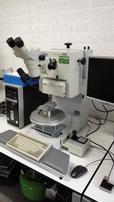
Bondtester by DAGE, in good condition. DAGE Series 4000 Bondtester product information. The 4000 bondtester is multipurpose, capable of performing all pull and shear applications. The 4000 bondtester can be configured as a simple bond wire pull
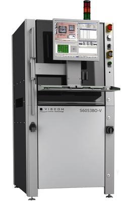
High accuracy inspection guarantees reliable defect detection of die bonds, ball-to-wedge, wedge-to-wedge and security bonds Inspection of minimal wire thicknesses up to 15 µm Reliable differentiation of wire courses Recognition of defective bon
Industry News | 2015-08-11 09:37:25.0
Saline Lectronics now offers wire bonding in-house as an added-value service. With the installation of the Kulicke & Soffa 4500 Manual Wedge Bonder, Saline Lectronics is now one of the only electronic contract manufacturers in the Midwest to support wire bonding services.


