Technical Library | 2022-10-31 18:35:40.0
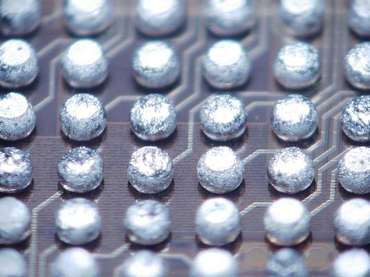
Voids affect the thermal characteristics and mechanical properties of a solder joint, thereby affecting the reliability of the solder interconnect. The automotive sector in particular is requiring the mitigation of solder voids in various electronic control modules to the minimum possible level. Earlier research efforts performed to decrease voids involved varying the reflow profile, paste deposit, paste alloy composition, stencil aperture, and thickness. Due to the various advantages they offer, the use of Ball Grid Array packages is common across all industry sectors. They are also prone to process voiding issues. This study was performed to determine if vacuum assisted reflow process can help alleviate the voids in area array solder joints. Test parameters in this study largely focused on vacuum pressure level and vacuum dwell time.
Industry News | 2022-09-05 06:50:46.0
The company will also unveil new WaferSense® and ReticleSense® Auto Teach Systems™ (ATS2™ and ATSR™)
Industry News | 2015-10-11 16:19:40.0
Photo Stencil announces that Susan Holmes, VP engineering and customer service for Photo Stencil, will present the paper Stencil Design for Wafer Level Ball Drop and Flip Chip Assembly at the IWLPC during Session 10 on Wednesday, October 14, 2015, at 5:00 PM. The 12th Annual International Wafer-Level Packaging Conference and Tabletop Exhibition is being held at the Doubletree San Jose Airport Hotel, San Jose, CA.
Industry Directory | Manufacturer
The exclusive supplier of SIPAD Solid Solder Deposit in North America and the only SIPAD Solid Solder Deposit (SSD) coating service bureau in the world.
Industry News | 2023-06-12 20:40:57.0
Atlanta, GA – Koh Young, the industry leader in True3D™ measurement-based inspection solutions, is pleased to announce its return to SEMICON West with a new series of inspection solutions designed to increase advanced package and semiconductor yield. Several of our latest inspection machines will be on display during SEMCION West in booth 329 from 11-13 July 2023 in the Moscone Center, San Francisco, CA.
New Equipment | Cleaning Agents
MICRONOX® MX2302 is an engineered semiaqueous solvent blend designed to remove difficult flux and paste residues including lead-free, rosin, no-clean, and tacky flux from wafer bumps found in flip chip, chip scale and μBGA packages. MICRONOX® MX2302
Industry News | 2021-11-05 07:26:32.0
Both Metrology and Inspection Systems are Powered by Advanced 3D Multi-Reflection Suppression™ (MRS™) Sensor Technology
Industry News | 2024-03-04 11:44:39.0
StenTech® Inc. has completed a major technology update to their Photo Stencil Specialized Products Division in Golden, Colorado. The phase-one overhaul included upgrades to key areas, including imaging, chemical plating, metrologymetrology, and chemical coating, along with refreshed offices and board room.

Virtual Panel Tooling provides just that: dozens of substrates are independently aligned, simultaneously, creating a virtual panel ready for imaging in a single cycle. This concept delivers high throughput comparable to processing panelised substrate
Industry News | 2010-06-21 16:04:54.0
Demonstrating its extensive knowledge base for today’s demanding back-end wafer level processes, DEK’s presence at the upcoming Semicon West event in San Francisco, California will feature the Galaxy print platform with Wafer Transport Solution. This system, displayed alongside the CHAD WaferMate 300-1, is configured with a precision wafer pallet and high-performance transport rails, ensuring the accuracy and stability required for DEK’s established and emerging cost-effective Wafer Level Packaging (WLP) applications.


