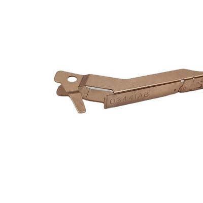
Parts & Supplies | Pick and Place/Feeders
Panasonic machine parts for sales Can offer the parts in original new, used or compatible condition. KXFB04WAA00 BRACKET N510017430AA BOLT N510030817AA URETHANE N510057134AA CYLINDER N610024683AA Conveyer Cover Opening(H=32mm) N610117727AA W
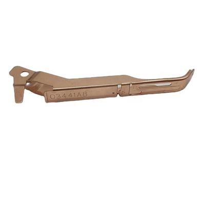
Parts & Supplies | Pick and Place/Feeders
Panasonic machine parts for sales Can offer the parts in original new, used or compatible condition. KXFB04WAA00 BRACKET N510017430AA BOLT N510030817AA URETHANE N510057134AA CYLINDER N610024683AA Conveyer Cover Opening(H=32mm) N610117727AA W

Used SMT Equipment | Pick and Place/Feeders
This Genesis Has been fully maintained with all Annuals performed by Universal Instruments. It is in outstanding condition and has the retrofit Vision Upgrade completed Universal. It is loaded with features here are some: * Model 4988F GI-14D Confi
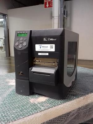
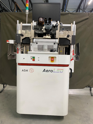
Used SMT Equipment | Labeling Systems
Zebra Technologies Z4M Thermal Barcode Label Printer Manufacturer: Zebra Technologies Model: Z4M Printer Type: Label printer Camera installed size: 2 MB Power device Type: power supply Nominal Voltage: AC 120/230 V Frequency Required: 50/6
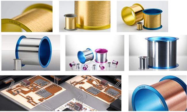
Gold / Aluminum / Copper Bonding Wires The bonding wires is the most important material used in making electrical connections between the chip and the external circuit. It has good conductivity and corrosion resistance, and it could be used for extr
Used SMT Equipment | Semiconductor & Solar
Standard Machine features and system description: Ultra-fine pitch and small ball bonding capabilities High frequency transducer operating at 138 kHz Applicable wire size of 0.6mil-2.0mil High speed XY table with linear motor technology High ac
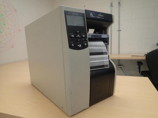
Used SMT Equipment | General Purpose Equipment
Zebra Xi Series 110Xi4 Thermal Barcode Label Printer GENERAL Manufacturer: Zebra Technologies Model: X1 Series 110Xi4 Printer Type:Label printer PRINTER Print Speed: Up to 840.9 inch/min - max speed Built-in Devices:peeler with liner rewind
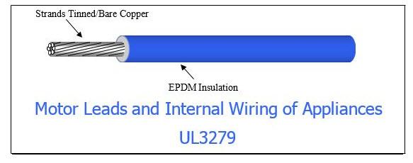
New Equipment | Cable & Wire Harness Equipment
Internal wiring of electronic equipment. Product Specification : Conductor material of Tinned or Bare copper Rated temperature 105℃ Rated Voltage 600 V (Spark voltage 6000 V) Flame resistance FT2 RoHS Compliant UL3279
Industry Directory | Manufacturer
Qualitetch utilse photo etching, wire EDM, laser cutting, metal forming, machining to offer the "Total Metal Component Solution" to customers requiring thin gauge metal components in most metals.
Technical Library | 2012-08-02 21:05:14.0
First published in the 2012 IPC APEX EXPO technical conference proceedings. Pure tin is a common finish for copper hook up wire, coaxial cable, ground braid and harness assemblies used on electronic assemblies. Historically there have been fewer reports o


