
Industry Directory | Consultant / Service Provider / Media / Publisher / Online Resource / Other
PCB Libraries' "Footprint Expert" suite uses CAD LEAP(tm) Technology to greatly simplify footprint and 3D STEP model creation; it is used by tens of thousands of PCB designers and engineers all over the world.
Industry Directory | Consultant / Service Provider / Manufacturer
A Top-25 global EMS provider headquartered in Burnaby, BC, Canada

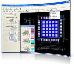
The PCB Footprint Expert is a powerful CAD library development tool powered by our own proprietary CAD LEAP Technology (Libraries Enhanced with Automated Preferences). It is packed with very powerful advanced library management features that cuts foo
New Equipment | Education/Training
IPC-7351B includes both the standard and an IPC-7351B land pattern calculator on CD-ROM for accessing component and land pattern dimensional data.The calculator includes the document’s mathematical algorithms so users can build a land pattern for a c
Electronics Forum | Wed Jun 19 16:39:22 EDT 2019 | travishemen
I think in the shape data on the shape process tab you click launch visual data editor.
Electronics Forum | Fri Oct 04 05:45:55 EDT 2019 | rajeshoshnic
Hi,You need Fuji VPD license for using image from camera stand. Thanks
Used SMT Equipment | Pick and Place/Feeders
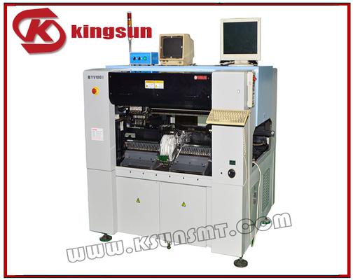
Product number: YV100 Ⅱ Products in detail YAMAHA multi-function chip mounter YAMAHA YV100II The brand YAMAHA model YV100 - II Automatic manual automatic SMT speed 10000(grain per hour) Japan's YAMAHA YV100II SMT machine: The patch speed: 0
Used SMT Equipment | Pick and Place/Feeders
Product number: YS88 Products in detail The characteristics of Configurable ~ 0402 chip - 55 mmcomponents, the wide range of special-shaped long joint element The height of the object elementcorresponds to 25.5 mm 10 ~ 30 n can be easy to stick
Industry News | 2003-03-21 08:12:24.0
Tecan reckons it is consistently producing what may be regarded as the most efficient stencils in the world today.
Industry News | 2018-02-01 02:56:53.0
More is not less, rather more is completely free. These newly released features were originally available to our enterprise-level customers, and now available at absolutely no cost, no obligation, no strings attached, to automate creation of tens of millions of parts...
Parts & Supplies | Repair/Rework
The RocHard 1 MilProbe is a 0.3" long Micro-tip in a 4 3/8" long hex shape stainless steel handle. The Micro-tip is tapered to a one mil diameter tip for TAB, BGA, and other ultra fine pitch rework. The tip is either straight (SH-341) or 50? angled a

Parts & Supplies | Assembly Accessories
Product name: YV100X YAMAHA multi-functional chip mounter Product number: YV100X Products in detail YAMAHA multi-function placement machineYAMAHA YV100X substrate size: ATS20 (end to put) W -AT assembly: L460 * W250 (Max)/L50 * W50 (Min)sub
Technical Library | 2024-02-02 07:48:31.0
Maximizing Efficiency: The High-Speed SMT Line With Laser Depanelizer In today's rapidly evolving electronics manufacturing landscape, optimizing efficiency, cost-effectiveness, and precision remains paramount. Businesses engaged in producing industrial control boards, computer motherboards, mobile phone motherboards, and mining machine boards face ongoing challenges in streamlining production processes. The integration of expensive equipment strains budgets, making the creation of an efficient, cost-effective high-speed SMT line a daunting task. However, a solution exists that seamlessly combines these elements into a singular, high-performance, and cost-effective SMT line. Let's delve into the specifics. A Comprehensive High-Speed SMT Line Our innovative solution amalgamates two pivotal components: a cutting-edge SMT (Surface Mount Technology) production line and a laser cutting line equipped with a depanelizer. The SMT Production Line The high-speed SMT line comprises several essential components, each fulfilling a unique role in the manufacturing process: 1. PCB Loader: This initial stage involves loading boards onto the production line with utmost care. Our Board Loader prioritizes safety, incorporating various safety light curtains and sensors to promptly halt operations and issue alerts in case of any anomalies. 2. Laser Marking Machine: Every PCB receives a unique two-dimensional code or barcode, facilitating comprehensive traceability. Despite the high-temperature laser process potentially leading to dust accumulation on PCB surfaces, our dedicated PCB Surface Cleaner swiftly addresses this issue. 3. SMT Solder Paste Printer: This stage involves applying solder paste to the boards, a fundamental step in the manufacturing process. 4. SPI (Solder Paste Inspection): Meticulous inspections are conducted at this stage. Boards passing inspection proceed through the NG (No Good) Buffer Conveyor to the module mounters. Conversely, "No Good" results prompt storage of PCBs in the NG Buffer Conveyor, capable of accommodating up to 25 PCBs. Operators can retrieve these NG boards for rework after utilizing our specialized PCB Mis Cleaner to remove solder paste. 5. Module Mounters: These machines excel in attaching small and delicate components, necessitating precision and expertise in the module mounting process. 6. Standard Pick And Place Machines: The selection of these machines is contingent upon your specific BOM (Bill of Materials) list. 7. Pre-Reflow AOI (Automated Optical Inspection): Boards undergo examination for component quality at this stage. Detected issues prompt the Sorting Conveyor to segregate boards for rework. 8. Reflow Oven: Boards undergo reflow soldering, with our Lyra series reflow ovens recommended for their outstanding features, including nitrogen capability, flux recycling, and water cooling function, ensuring impeccable soldering results. 9. Post-Reflow AOI: This stage focuses on examining soldering quality. Detected defects prompt the Sorting Conveyor to segregate boards for further inspection or rework. Any identified defects are efficiently addressed with the BGA rework station, maintaining the highest quality standards. 10. Laser Depanelizer: Boards advance to the laser depanelizer, where precision laser cutting, often employing green light for optimal results, ensures smoke-free, highly accurate separation of boards. 11. PCB Placement Machine: Cut boards are subsequently managed by the PCB Placement Machine, arranging them as required. With this, all high-speed SMT line processes are concluded. Efficiency And Output This production line demonstrates exceptional productivity when manufacturing motherboards with approximately 3000 electronic components, boasting the potential to assemble up to 180 boards within a single hour. Such efficiency not only enhances output but also ensures cost-effectiveness and precision in your manufacturing processes. At I.C.T, we specialize in crafting customized SMT production line solutions tailored to your product and specific requirements. Our equipment complies with European safety standards and holds CE certificates. For inquiries or to explore our exemplary post-sales support, do not hesitate to contact us. The I.C.T team is here to elevate your electronics manufacturing to new heights of efficiency and cost-effectiveness.
Technical Library | 2020-10-30 10:27:39.0
Preview of the Complete Aneryn's Orbotech Trion 2340 Manual. It explains how to programme the AOI machine, how to train new components (shapes), how to connect it to your network, among other processes. Following the Guide, you will minimize false alarms and escapes rates easily. Full Manual available at https://aneryn.com/creation/trion-2340-manual/ Digital development by Sinfonía Digital

The PCB Footprint Expert is a powerful CAD library development tool powered by our own proprietary CAD LEAP Technology (Libraries Enhanced with Automated Preferences). It is packed with very powerful advanced library management features that cuts foo
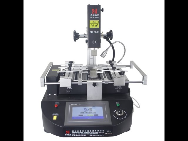
Condition: New Machine Type: BGA rework station Applicable Industries: Machinery Repair Shops, Manufacturing Plant, Retail After Warranty Service: Video technical support, Online support, Spare parts Video outgoing-inspection: Provided Machinery
Training Courses | | | PCB Design Courses
The PCB design courses teach students the process, techniques and tools needed to design layout of printed circuit boards.
Training Courses | | | PCB Design Courses
The PCB design courses teach students the process, techniques and tools needed to design layout of printed circuit boards.
Career Center | Williamsport, Pennsylvania USA | Engineering,Quality Control
Spartronics is more than just a company. We have great facilities, a dedicated and talented team, tremendous capacity and capabilities, and longstanding customers who need us. Now, it’s all about driving forward with a winning strategy that bui
Career Center | Strongsville, Ohio USA | Engineering,Quality Control
Spartronics is more than just a company. We have great facilities, a dedicated and talented team, tremendous capacity and capabilities, and longstanding customers who need us. Now, it’s all about driving forward with a winning strategy that bui
Career Center | brampton, Ontario Canada | Engineering,Management,Production,Technical Support
- More than 14 years of experience in set-up, calibrate, program, troubleshoot SMT machines and SMT process, for the manufacturing of PCB Electronic Assemblies - 5 year experience in leading position for electronic manufacturing/Process Engineering.
Career Center | Erode, Tamilnadu India | Engineering
Professional Summary 3+ years of experience in the PCB CAM engineering Exposure to FRONTLINE GENESIS 2000 Having exposure in UCAM Exposure to Create, Array & Panelize it for manufacturability Experienced in Creating impedance cou
Heller Industries Inc. | https://hellerindustries.com/wp-content/uploads/2018/07/last-will-of-bga-void.pdf
particular BGA row. Black areas represent voids/cracks. The location, size and shape of the voids can be precisely examined. The cracks resulting from the thermal cycling are also clearly visible. Once the CT model is compiled the failure analysis engineer
Imagineering, Inc. | https://www.pcbnet.com/blog/hdi-pcb-advantages-and-applications/
. This type of PCB technology allows for improved functionality in smaller consumer products, denser BGA and QFP packages, and lowered heat transfer induced stress


