Industry Directory | Manufacturer
Shuttle Star Technology designs and builds advanced off-line 2.5D&3D x-ray inspection systems for solder joint and final assembly test inspection in SMT&EMS. It uses world-class X-ray techniques with advanced defect detection.
Industry Directory | Manufacturer
Manufacturer of materials for the electronics assembly marketplace. Our RoHS-compliant products include solder pastes, fluxes, solder powder, core wire and bar solder and process support products.

The I.C.T X-7100 is a high-performance automatic offline X-ray inspection machine, designed for precise non-destructive testing (NDT) of SMT PCB assemblies, semiconductor components, and BGA/void detection. This system provides high-resolution X-ray
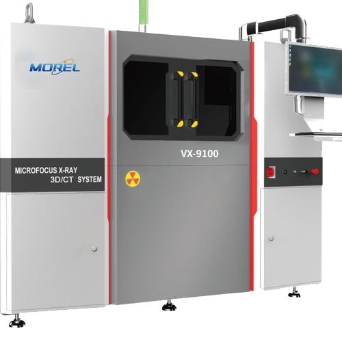
MICROFOCUS X-RAY 3D/CT SYSTEM VX-9100 The VX-9100 3D X-Ray Inspection Machine is a state-of-the-art industrial microfocus CT system designed for precise quality inspection and non-destructive analysis of electronic components. Its advanced cap
Electronics Forum | Thu Apr 23 22:01:07 EDT 2009 | davef
That you have one BGA of 30 BGA that has voids, makes us wonder what's the deal with that one BGA. Especially given that this is the initial run of a product with BGA at your plant, it really makes us want to understand just what is driving the voidi
Electronics Forum | Mon Jan 13 16:23:29 EST 2003 | Eric Brown
Does anyone know of documentation that specifies whether or not voids in BGA solder joints hurt or help performance?
Used SMT Equipment | X-Ray Inspection
we are looking for wth following options: Automatic microfocus X-ray inspection system including: - 160 kV proprietary microfocus X-ray source (open design) with “unlimited” lifetime, including demountable collimator for enhanced image qualit

Used SMT Equipment | X-Ray Inspection
• Installed new in 2006 • Single Owner and used in a Lab Environment • Maintained by OEM and under OEM ASC, throughout original ownership • Currently offline and immediately available Tube Type: 160kv NF – Transmissive type (open tube ~ maintain
Industry News | 2016-01-17 19:26:58.0
In order to keep up with industry demand, IPC has released amendments for J-STD-001F, Requirements for Soldered Electrical and Electronic Assemblies, and IPC-A-610F, Acceptability of Electronic Assemblies. For each standard, IPC-A-610F Amendment 1 and IPC J-STD-001F Amendment 1 represents a critical shift to deliver necessary updates to these already robust standards.
Industry News | 2018-10-18 08:17:09.0
How to Prevent Solder Joint Voiding and Cold Solder Defects during the SMT Reflow Process

Parts & Supplies | Repair/Rework
. This machine adopts industrial computer control, full automatic vision alignment system can acquire BGA and the PCB image through the CCD camera and collect them on the image positioning processing system, calculate the offset position and angle th
Technical Library | 2023-01-17 17:22:28.0
The impact of voiding on the solder joint integrity of ball grid arrays (BGAs)/chip scale packages (CSPs) can be a topic of lengthy and energetic discussion. Detailed industry investigations have shown that voids have little effect on solder joint integrity unless they fall into specific location/geometry configurations. These investigations have focused on thermal cycle testing at 0°C-100°C, which is typically used to evaluate commercial electronic products. This paper documents an investigation to determine the impact of voids in BGA and CSP components using thermal cycle testing (-55°C to +125°C) in accordance with the IPC- 9701 specification for tin/lead solder alloys. This temperature range is more typical of military and other high performance product use environments. A proposed BGA void requirement revision for the IPC-JSTD-001 specification will be extracted from the results analysis.
Technical Library | 2015-01-05 17:38:26.0
The impact of voiding on the solder joint integrity of ball grid arrays (BGAs)/chip scale packages (CSPs) can be a topic of lengthy and energetic discussion. Detailed industry investigations have shown that voids have little effect on solder joint integrity unless they fall into specific location/geometry configurations. These investigations have focused on thermal cycle testing at 0°C-100°C, which is typically used to evaluate commercial electronic products. This paper documents an investigation to determine the impact of voids in BGA and CSP components using thermal cycle testing (-55°C to +125°C) in accordance with the IPC-9701 specification for tin/lead solder alloys. This temperature range is more typical of military and other high performance product use environments. A proposed BGA void requirement revision for the IPC-JSTD-001 specification will be extracted from the results analysis.

· What is the difference between SMT vacuum reflow soldering machine and ordinary reflow soldering machine? · What problems can be solved by smt vacuum reflow soldering machine? · What is the basic principle of vacuum reflow machine? · Ho

ACI Technologies Inc. (ACI) is a scientific research corporation dedicated to the advancement of electronics manufacturing processes and materials for The Department of Defense and industry. This video provides an overview of our commercial service
Training Courses | | | PCB Rework and Hand Soldering Courses
The PCB rework and hand soldering courses courses cover techniques of rework and repair of PCBs, BGAs and other electronics assemblies, and teach fundamentals of soldering of electronics assemblies.
Training Courses | | | PCB Rework and Hand Soldering Courses
The PCB rework and hand soldering courses courses cover techniques of rework and repair of PCBs, BGAs and other electronics assemblies, and teach fundamentals of soldering of electronics assemblies.
Events Calendar | Tue Feb 12 00:00:00 EST 2019 - Tue Feb 12 00:00:00 EST 2019 | ,
Webinar: BGA and Area Array Process Defects - Causes & Cures
Events Calendar | Mon Mar 16 00:00:00 EDT 2020 - Mon Mar 16 00:00:00 EDT 2020 | ,
BGA & Area Array Failures, Causes & Corrective Actions Online Webinar
Career Center | Erode, Tamilnadu India | Engineering
Professional Summary 3+ years of experience in the PCB CAM engineering Exposure to FRONTLINE GENESIS 2000 Having exposure in UCAM Exposure to Create, Array & Panelize it for manufacturability Experienced in Creating impedance cou
Career Center | Lakewood, California USA | Engineering,Maintenance,Management,Production
Quality conscience, detail oriented, manufacturing engineer, with a hands on approach to overall process improvement and development. Motivated with excellent communication skills and a dedicated team player. Qualifications include: � Safety /Diver
Voiding Control for QFN Assembly Voiding Control for QFN Assembly Quad Flat No Leads (QFN) package designs receive more and more attention in electronic industry nowadays. This package offers a number of benefits including (1) small size
PCB Libraries, Inc. | https://www.pcblibraries.com/Forum/bga-pad-size_topic2607_post10645.html
: 05 Jan 2012 Location: San Diego, CA Status: Offline Points: 5184 Post Options Post Reply Quote Tom H Report Post Thanks(0) Quote Reply Posted: 27 Feb 2020 at 11:31am The IPC mathematical model uses this table to calculate BGA pad stacks, but the Library Expert Preferences allows the User to change the values to whatever works best for you
Heller Industries Inc. | https://hellerindustries.com/wp-content/uploads/2018/07/last-will-of-bga-void.pdf
. This paper documents an investigation to determine the impact of voids in BGA and CSP components using thermal cycle testing (-55°C to +125°C) in accordance with the IPC- 9701 specification for tin/lead solder alloys


