Industry News | 2017-09-28 20:06:38.0
In cooperation with productronica 2017, IPC — Association Connecting Electronics Industries® is presenting its very popular Hand Soldering Competition in Hall A1, stand 307 at this year’s event. Skilled competitors will demonstrate their soldering skills, on 14 – 16 November, as they compete for cash prizes: 1st place — €300; 2nd place — €200; 3rd place — €100. New this year, IPC will feature the World Hand Soldering Championship on 17 November, 2017, with the regional winner from productronica and competitors from around the world. The winners of the IPC HSC World Championship will receive cash awards amounting to: 1000€ to the winner, 500€ for the runner up and 300€ for third place. The awards will be presented Friday, 17 November at 14:00 in the SMT speakers corner Hall A1, stand 220.
This video describes the IPC A-600 training and certification program. The IPC A-600 specification is a set of acceptability specifications for printed circuit boards. These standards determine the acceptance and reject criteria for printed wiring bo
New Equipment | Solder Paste Stencils
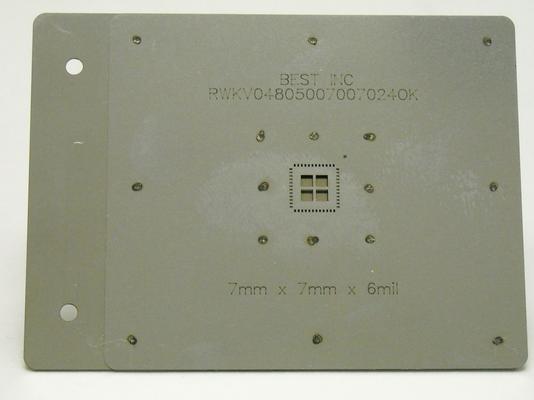
Based on its long work on BGA rework and repair process and its in-house capability to produce metal stencils BEST can provide for you a timely, cost-effective solution for printing on to components for MOST rework systems. Our templates for printin
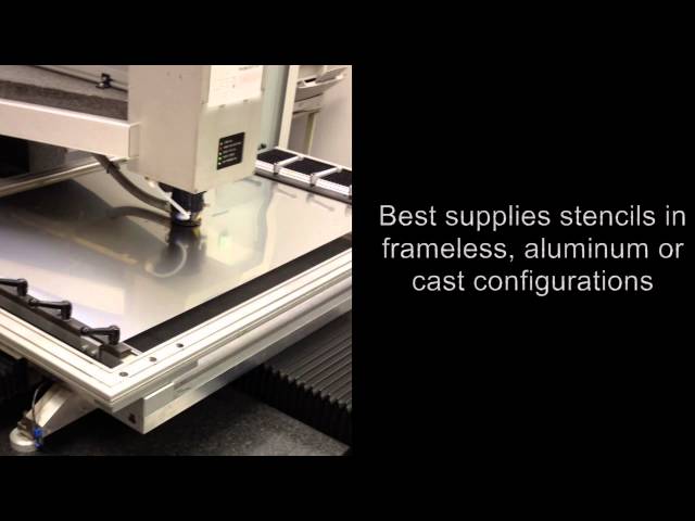
BEST manufactures and designs SMT stencils-both metal and plastic film type. This video demonstrates our metal stencil laser. See more on stencils here: http://www.soldertools.net/categories/Metal-Stencils/
BEST manufactures and designs SMT stencils-both metal and plastic film type. This video demonstrates our metal stencil laser. See more on stencils here: http://www.soldertools.net/categories/Metal-Stencils/
BEST manufactures and designs SMT stencils-both metal and plastic film type. This video demonstrates our metal stencil laser. See more on stencils here: http://www.soldertools.net/categories/Metal-Stencils/
New Equipment | Assembly Services
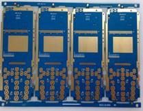
We are Professional in PCB Manufacturing, PCB Fabrication, PCB Making! Hitech Circuits Co., Limited – Experienced PCB manufacturer from China. Our PCB manufacturing services will allow you to be the most competitive player in your market. Please che
Technical Library | 2023-01-10 20:15:42.0
Over the past years there has been consistent growth in the use of electroless nickel / immersion gold (ENIG) as a final finish. The finish is now frequently being used for PBGA, CSP, QFP and COB and more recently gathered considerable interest as a low cost under-bump metallization for flip chip bumping application. One of the largest users for this finish has been the telecommunication industry, were millions of square meters of PCBs with ENIG have been successfully used. The nickel layer offers advantages such as multiple soldering cycles and hand reworks without copper dissolution being a factor. The nickel also acts as a reinforcement to improve through-hole and blind micro via thermal integrity. In addition the nickel layer offers advantages such as co-planarity, Al-wire bondability and the use as contact surface for keypads or contact switching. Especially those pads, which are not covered by solder need a protective coating in corrosive environment – such as high humidity or pollutant gas.
Technical Library | 2019-07-17 17:56:34.0
The increased demand for electronic devices in recent years has led to an extensive research in the field to meet the requirements of the industry. Electrolytic copper has been an important technology in the fabrication of PCBs and semiconductors. Aqueous sulfuric acid baths are explored for filling or building up with copper structures like blind micro vias (BMV), trenches, through holes (TH), and pillar bumps. As circuit miniaturization continues, developing a process that simultaneously fills vias and plates TH with various sizes and aspect ratios, while minimizing the surface copper thickness is critical. Filling BMV and plating TH at the same time, presents great difficulties for the PCB manufactures. The conventional copper plating processes that provide good via fill and leveling of the deposit tend to worsen the throwing power (TP) of the electroplating bath. TP is defined as the ratio of the deposit copper thickness in the center of the through hole to its thickness at the surface. In this paper an optimization of recently developed innovative, one step acid copper plating technology for filling vias with a minimal surface thickness and plating through holes is presented.
We manufacture multi PCB up to 12 layer,The details of our capabilities:*Micro fine line to 4 mil *Blind & buried via hole *Flying-probe testing *Carbonlack *FR4 thickness: 0.3/0.4/0.8/1.0/1.2/1.5/2.0/2.4/3.2mm *Small quantities are available *Golden finger *HAL & chemical tin


