New Equipment | Fabrication Services
Our Service PCB Assembly and PCB&PCBA design are our main business.We are able to undertake a high quality Printed Circuit Board Assembly on competitive prices and flexible conditions.We are a complete “One- Stop” resource for printed circuit board
New Equipment | Fabrication Services
Minimum line width/space: 4mils Surface finish: immersion gold Board thickness: 1.60MM Minimum drilled hole diameter: 4mils Copper thickness: 0.5oz Special process : 0.25MM BGA , resin plugged vias in BGA pads
.png)
Micor focus X-ray inspection , X-ray chip counter, Bga rework station, contact Rita Li by: Skype:ritaleeli whatsapp:0086 134 3448 1030 Email:sales11@zhuomao.com.cn Product Application: X-Ray inspection is a method of non-destructive testin
Technical Library | 2023-01-10 20:15:42.0
Over the past years there has been consistent growth in the use of electroless nickel / immersion gold (ENIG) as a final finish. The finish is now frequently being used for PBGA, CSP, QFP and COB and more recently gathered considerable interest as a low cost under-bump metallization for flip chip bumping application. One of the largest users for this finish has been the telecommunication industry, were millions of square meters of PCBs with ENIG have been successfully used. The nickel layer offers advantages such as multiple soldering cycles and hand reworks without copper dissolution being a factor. The nickel also acts as a reinforcement to improve through-hole and blind micro via thermal integrity. In addition the nickel layer offers advantages such as co-planarity, Al-wire bondability and the use as contact surface for keypads or contact switching. Especially those pads, which are not covered by solder need a protective coating in corrosive environment – such as high humidity or pollutant gas.
Technical Library | 2019-07-17 17:56:34.0
The increased demand for electronic devices in recent years has led to an extensive research in the field to meet the requirements of the industry. Electrolytic copper has been an important technology in the fabrication of PCBs and semiconductors. Aqueous sulfuric acid baths are explored for filling or building up with copper structures like blind micro vias (BMV), trenches, through holes (TH), and pillar bumps. As circuit miniaturization continues, developing a process that simultaneously fills vias and plates TH with various sizes and aspect ratios, while minimizing the surface copper thickness is critical. Filling BMV and plating TH at the same time, presents great difficulties for the PCB manufactures. The conventional copper plating processes that provide good via fill and leveling of the deposit tend to worsen the throwing power (TP) of the electroplating bath. TP is defined as the ratio of the deposit copper thickness in the center of the through hole to its thickness at the surface. In this paper an optimization of recently developed innovative, one step acid copper plating technology for filling vias with a minimal surface thickness and plating through holes is presented.
We manufacture multi PCB up to 12 layer,The details of our capabilities:*Micro fine line to 4 mil *Blind & buried via hole *Flying-probe testing *Carbonlack *FR4 thickness: 0.3/0.4/0.8/1.0/1.2/1.5/2.0/2.4/3.2mm *Small quantities are available *Golden finger *HAL & chemical tin
Industry Directory | Manufacturer
UWELLPCB.com is the PCB supplier. We offer PCB from single side board, double side PCB to 32layer board,including the Rigid PCB, Flex PCB, Rigid-flex PCB,Quick-turn prototype and PCB assembly

Parts & Supplies | Circuit Board Assembly Products
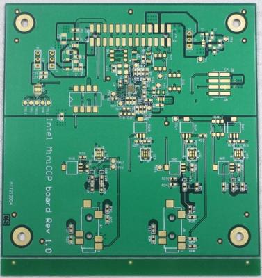
1). 80 *190mm/2up, FR-4 2). 6 layers at 1.4mm thick 3). 35 μm copper weight 4). Green solder mask LPI/White legend 5). ENIG surface finish 6). Blind via from Layer 1 to layer 2 7). Via in pad plugged conductive resin
Industry Directory | Manufacturer
A printed circuit board manufacturer producing high quality prototype printed circuit boards.
Double-Sided & Multi-Layer PCB Material: - FR-4 / Hi-Temp FR-4 / FR-5 / G10 / BT / Polyimide - Very Thin PCB: 0.004" 2L ~ 0.030" 8L - Thick Copper: 1/4 oz. ~ 11 oz. Process: - PTH - Blind/Buried/Segmented Via - Sequential Lamination - MicroVia Capa


