Industry Directory | Manufacturer's Representative
AlSi BondPads for PCB and Hybrid Packaging modules
Industry Directory | Manufacturer
Nepes offers flip chip solutions ranging from wafer bumping to advanced packaging and testing for IC manufactures, module electronics and end-product makers.

We are well versed in the following thermal application materials: Sil-Pad thermally conductive insulators Gap-Pad thermally conductive gap filling material Q-Pad thermal grease replacement film Bond-Ply thermally conductive adh
Complex functions are compressed on ever less room while simultaneously an enhancement in performance must be obtained. With coated Bonding pads in various designs Heraeus Materials Technology offers customer oriented solutions that aid the increas
Electronics Forum | Fri Dec 16 13:37:52 EST 2016 | edhare
Hi all, > > Recently, we are trying to do > wire bonding between a 75 * 75 um pad on a chip > and substrate with 150 um height difference, but > when completing wire bonding and the wire bonds > on pad and substrate, the pad will get out of
Electronics Forum | Wed Dec 14 12:34:56 EST 2016 | cy4223111
Hi all, Recently, we are trying to do wire bonding between a 75 * 75 um pad on a chip and substrate with 150 um height difference, but when completing wire bonding and the wire bonds on pad and substrate, the pad will get out of the chip easily
Industry News | 2003-02-24 09:32:24.0
Now available with an easy-to-use dispensing gun, Electrolube TCR is a single-component, highly thermally conductive RTV sealant.
Industry News | 2004-09-07 18:32:13.0
NORTHBROOK, Ill., September, 2004

Parts & Supplies | Pick and Place/Feeders
The definition of SMT SMT is the surface assembly technology,surface mount technology(surface mount technology)(Surface Mounted Technology abbreviation),is currently the most popular electronic assembly industry,a technology and technology. What a
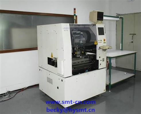
Parts & Supplies | Pick and Place/Feeders
SMT basic process components include: silk screen (or dispensing), placement (curing), reflow soldering, cleaning, testing, repair 1, silk screen: its role is to paste or patch solder paste printed on the PCB pad, the components f
Technical Library | 2017-08-31 13:43:48.0
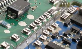
Wire bonded packages using conventional copper leadframe have been used in industry for quite some time. The growth of portable and wireless products is driving the miniaturization of packages resulting in the development of many types of thin form factor packages and cost effective assembly processes. Proper optimization of wire bond parameters and machine settings are essential for good yields. Wire bond process can generate a variety of defects such as lifted bond, cracked metallization, poor intermetallic etc. NSOP – non-stick on pad is a defect in wire bonding which can affect front end assembly yields. In this condition, the imprint of the bond is left on the bond pad without the wire being attached. NSOP failures are costly as the entire device is rejected if there is one such failure on any bond pad. The paper presents some of the failure modes observed and the efforts to address NSOP reduction
Technical Library | 2020-08-27 01:22:45.0
Initially adopted internal specifications for acceptance of printed circuit boards (PCBs) used for wire bonding was that there were no nodules or scratches allowed on the wirebond pads when inspected under 20X magnification. The nodules and scratches were not defined by measurable dimensions and were considered to be unacceptable if there was any sign of a visual blemish on wire-bondable features. Analysis of the yield at a PCB manufacturer monitored monthly for over two years indicated that the target yield could not be achieved, and the main reasons for yield loss were due to nodules and scratches on the wirebonding pads. The PCB manufacturer attempted to eliminate nodules and scratches. First, a light-scrubbing step was added after electroless copper plating to remove any co-deposited fine particles that acted as a seed for nodules at the time of copper plating. Then, the electrolytic copper plating tank was emptied, fully cleaned, and filtered to eliminate the possibility of co-deposited particles in the electroplating process. Both actions greatly reduced the density of the nodules but did not fully eliminate them. Even though there was only one nodule on any wire-bonding pad, the board was still considered a reject. To reduce scratches on wirebonding pads, the PCB manufacturer utilized foam trays after routing the boards so that they did not make direct contact with other boards. This action significantly reduced the scratches on wire-bonding pads, even though some isolated scratches still appeared from time to time, which caused the boards to be rejected. Even with these significant improvements, the target yield remained unachievable. Another approach was then taken to consider if wire bonding could be successfully performed over nodules and scratches and if there was a dimensional threshold where wire bonding could be successful. A gold ball bonding process called either stand-off-stitch bonding (SSB) or ball-stitch-on-ball bonding (BSOB) was used to determine the effects of nodules and scratches on wire bonds. The dimension of nodules, including height, and the size of scratches, including width, were measured before wire bonding. Wire bonding was then performed directly on various sizes of nodules and scratches on the bonding pad, and the evaluation of wire bonds was conducted using wire pull tests before and after reliability testing. Based on the results of the wire-bonding evaluation, the internal specification for nodules and scratches for wirebondable PCBs was modified to allow nodules and scratches with a certain height and a width limitation compared to initially adopted internal specifications of no nodules and no scratches. Such an approach resulted in improved yield at the PCB manufacturer.

ACI Technologies Inc. (ACI) is a scientific research corporation dedicated to the advancement of electronics manufacturing processes and materials for The Department of Defense and industry. This video provides an overview of our commercial service

PCB pad repair technique demonstrated using the 2-part epoxy method. More on this PCB pad repair technique: http://www.solder.net/services/pcb-repair/pad-and-trace-repair/ More on the recommended epoxy: http://www.soldertools.net/pcb-repair-epoxy-r
Training Courses | | | IPC-7711/7721 Specialist (CIS)
The Certified IPC-7711/7721 Specialist (CIS) training focuses on rework of electronic assemblies and repair and modification of printed boards and electronic assemblies.
Training Courses | | | IPC-7711/7721 Trainer (CIT)
The Certified IPC-7711/7721 Trainer (CIT) courses recognize individuals as qualified trainers in the area of rework and repair of printed boards and electronic assemblies and prepares them to deliver Certified IPC-7711/7721 (CIS) training.
Events Calendar | Mon Apr 23 00:00:00 EDT 2018 - Thu Apr 26 00:00:00 EDT 2018 | Shanghai, China
SMTA China East Conference 2018
Events Calendar | Tue Dec 04 00:00:00 EST 2018 - Tue Dec 04 00:00:00 EST 2018 | ,
Qualification and Reliability of Microvias
SMT Express, Volume 2, Issue No. 9 - from SMTnet.com Volume 2, Issue No. 9 Thursday, September 14, 2000 Featured Article Return to Front Page Book Review Reviewed by Dave Fish (davef ), Pandion Electronics, Inc Title: Wire Bonding
SMTnet Express, August 31, 2017, Subscribers: 30,770, Companies: 10,706, Users: 23,739 NSOP Reduction for QFN RFIC Packages Mumtaz Y. Bora; Peregrine Semiconductor Wire bonded packages using conventional copper leadframe have been used in industry
ASYMTEK Products | Nordson Electronics Solutions | https://www.nordson.com/en/divisions/dage/about/news/nordson-dage-announces-further-orders-for-its-unique-patented-hot-pin-pull-test-method
” testing which involves attaching a test probe to an individual solder ball with a controlled temperate / time profile. Once cooled the probe is subjected to a pull test which applies a test load that is symmetrical to the solder ball attach to the bonding pad
| https://www.eptac.com/faqs/ask-helena-leo/ask/gold-wire-bond-failing-pull-test
) Beam broken between bond and edge of silicon. (d-6) Bond lifted. (d-7) Lifted metallization (separation of metallization) from die, separation of bonding pad. (d-8
winsouce.jpg)
.gif)

