Industry News | 2015-11-25 16:58:05.0
On behalf of the SMTA International Technical Committee, we invite you to submit a 300 word abstract of your research for the 2016 SMTA International 2016 technical conference in Rosemont, Illinois. Papers should describe significant results from experiments, emphasize new techniques, and contain technical, economic or appropriate test data. We are looking for papers on a variety of topics related to electronics manufacturing including advanced packaging/components, assembly, business/supply chain, emerging technologies, harsh environment applications, PCB technology, and process control. Materials must be original, unpublished and non-commercial in nature.

The PCB Footprint Expert is a powerful CAD library development tool powered by our own proprietary CAD LEAP Technology (Libraries Enhanced with Automated Preferences). It is packed with very powerful advanced library management features that cuts foo
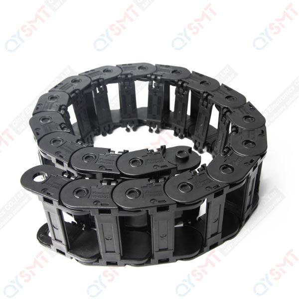
Parts & Supplies | Pick and Place/Feeders
We also supply following JUKI spare parts: 40000403 ADJUST BOLT 40000404 ADJUST BOLT(EN) 40000405 CASTER 40000411 Y-AXIS SENSOR BR ASSY 40000413 FEEDER FLOAT_SENS ASSY 40000414 FEEDER_SENS ASSY 40000419 CONTROL UNIT(60) 40000431 PANEL
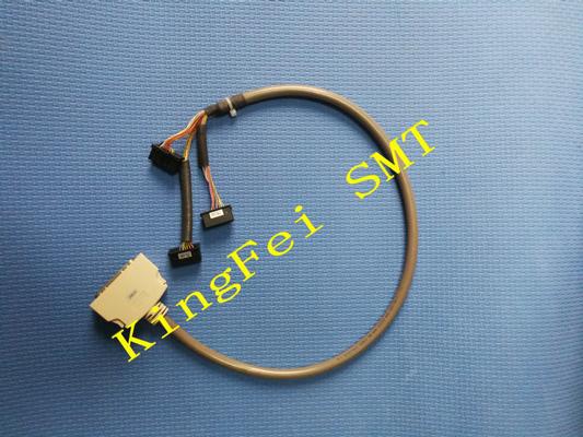
Parts & Supplies | Assembly Accessories
Detailed Product Description Part Name: LNC60 I/F Cable ASM Part Number: 40070445 Machine: JUKI KE2070 2080 FX3 Machine Condition: Original New Brand: JUKI Application: For LNC60 Laser 40070445 LNC60 I/F Cable ASM(2012) For JUKI 2070 2080 FX3 Mac
Technical Library | 2017-07-20 15:18:15.0
As electronic devices increase functionality in smaller form factors, there will be limitations, obstacles and challenges to overcome. Advances in component technology can create issues that may have time delayed effects. One such effect is device failure due to soldering residues trapped under bottom terminated components. If the residues trapped under the component termination are active and can be mobilized with moisture, there is the potential for ion mobilization causing current leakage.
Technical Library | 2014-10-23 18:10:10.0
The functional reliability of electronic circuits determines the overall reliability of the product in which the final products are used. Market forces including more functionality in smaller components, no-clean lead-free solder technologies, competitive forces and automated assembly create process challenges. Cleanliness under the bottom terminations must be maintained in harsh environments. Residues under components can attract moisture and lead to leakage currents and the potential for electrochemical migration (...) The purpose of this research study is to evaluate innovative spray and soak methods for removing low residue flux residues and thoroughly rinsing under Bottom Termination and Leadless Components
Technical Library | 2015-07-14 13:19:10.0
Bottom terminated components (BTC) are leadless components where terminations are protectively plated on the underside of the package. They are all slightly different and have different names, such as QFN (quad flat no lead), DFN (dual flat no lead), LGA (land grid array) and MLF (micro lead-frame. BTC assembly has increased rapidly in recent years. This type of package is attractive due to its low cost and good performance like improved signal speeds and enhanced thermal performance. However, bottom terminated components do not have any leads to absorb the stress and strain on the solder joints. It relies on the correct amount of solder deposited during the assembly process for having a good solder joint quality and reliable reliability. Voiding is typically seen on the BTC solder joint, especially on the thermal pad of the component. Voiding creates a major concern on BTC component’s solder joint reliability. There is no current industry standard on the voiding criteria for bottom terminated component. The impact of voiding on solder joint reliability and the impact of voiding on the heat transfer characteristics at BTC component are not well understood. This paper will present some data to address these concerns.
Technical Library | 2018-05-23 12:12:43.0
Driven by miniaturization, cost reduction and tighter requirements for electrical and thermal performance, the use of lead-frame based bottom-termination components (LF-BTC) as small-outline no-leads (SON), quad-flat no leads (QFN) packages etc., is increasing. However, a major distractor for the use of such packages in high-reliability applications has been the lack of a visible solder (toe) fillet on the edge surface of the pins: because the post-package assembly singulation process typically leaves bare copper leadframe at the singulation edge, which is not protected against oxidation and thus does not easily solder-wet, a solder fillet (toe fillet) does not generally develop.
Technical Library | 2020-12-29 20:55:46.0
Voiding in solder joints has been studied extensively, and the effects of many variables compared and contrasted with respect to voiding performance. Solder paste flux, solder powder size, stencil design, circuit board design, via-in-pad design, surface finish, component size, reflow profile, vacuum reflow, nitrogen reflow and other parameters have been varied and voiding quantified for each. The results show some differences in voiding performance with respect to most of these variables but these variables are not independent of each other. Voiding in solder joints is a complex issue that often requires multiple approaches to reduce voiding below required limits. This paper focuses on solutions to voiding for commonly used bottom terminated components (BTCs).
Technical Library | 2023-09-18 14:10:01.0
As with many advancements in the electronics industry, consumer electronics is driving the trends for electronic packaging technologies toward reducing size and increasing functionality. Microelectronics meeting the technology needs for higher performance, reduced power consumption and size, and off the- shelf availability. Due to the breadth of work being performed in the area of microelectronics packaging/components, this report limits it presentation to board design, manufacturing, and processing parameters on assembly reliability for leadless (e.g., quad flat no-lead (QFN) or a generic term of bottom termination component (BTC)) packages. This style of package was selected for investigation because of its significant growth, lower cost, and improved functionality, especially for use in an RF application.


