New Equipment | Rework & Repair Equipment
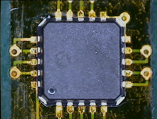
This is a unique stenciling BTC (QFN , LGS, etc) rework stencil system. It improves first pass yields and allows you to rework leadless devices without high-end rework systems. This configurable part number means you do not have to sort through all

QFN stenicl bumping process demonstrated using a polyimide stencil. This process is one in which a stencil is used to the bump the bottom terminations of a leadless device making it simple to place without voiding of the the thermal pac or shorting o
New Equipment | Solder Materials
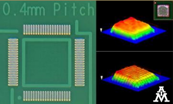
90% on area ratios of 0.50 and a stencil life >8 hours. H10’s powerful wetting characteristics eliminate NWO (HiP) defects and improve pad coverage on all surface finishes. H10 reduces voiding on BGA, BTC and LGA and offers enhanced electrochemical r
Technical Library | 2019-05-22 21:24:05.0
voidless treatment Smaller components -> miniaturization (01005 capability) Large board handling -> dynamic preheating for large board repair Repeatable processes -> flux and paste application (Dip and Print), residual solder removal (scavenging), dispensing, multiple component handling, and traceability Operator support -> higher automation, software guidance
Technical Library | 2015-07-14 13:19:10.0
Bottom terminated components (BTC) are leadless components where terminations are protectively plated on the underside of the package. They are all slightly different and have different names, such as QFN (quad flat no lead), DFN (dual flat no lead), LGA (land grid array) and MLF (micro lead-frame. BTC assembly has increased rapidly in recent years. This type of package is attractive due to its low cost and good performance like improved signal speeds and enhanced thermal performance. However, bottom terminated components do not have any leads to absorb the stress and strain on the solder joints. It relies on the correct amount of solder deposited during the assembly process for having a good solder joint quality and reliable reliability. Voiding is typically seen on the BTC solder joint, especially on the thermal pad of the component. Voiding creates a major concern on BTC component’s solder joint reliability. There is no current industry standard on the voiding criteria for bottom terminated component. The impact of voiding on solder joint reliability and the impact of voiding on the heat transfer characteristics at BTC component are not well understood. This paper will present some data to address these concerns.
Used SMT Equipment | General Purpose Equipment
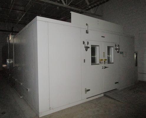
Espec Panelized EWPT 3468 - CCW Walk-In Temperature Chamber Brand: Espec Model: EWPT 3468 - CCW Serial#: 305536 Vintage: 2003 Power: 460V 3PH 60Hz. Temperature Control System: Balanced Temperature Control System: BTC Ambient Temperature:
Technical Library | 2013-07-25 14:02:15.0
Bottom-termination components (BTC), such as QFNs, are becoming more common in PCB assemblies. These components are characterized by hidden solder joints. How are defects on hidden DFN joints detected? Certainly, insufficient solder joints on BTCs cannot be detected by manual visual inspection. Nor can this type of defect be detected by automated optical inspection; the joint is hidden by the component body. Defects such as insufficients are often referred to as "marginal" defects because there is likely enough solder present to make contact between the termination on the bottom-side of the component and the board pad for the component to pass in-circuit and functional test. Should the board be subjected to shock or vibration, however, there is a good chance this solder connection will fracture, leading to an open connection.
Technical Library | 2015-06-11 21:20:29.0
The use of bottom terminated components (BTC) has become widespread, specifically the use of Quad Flat No-lead (QFN) packages. The small outline and low height of this package type, improved electrical and thermal performance relative to older packaging technology, and low cost make the QFN/BTC attractive for many applications.Over the past 15 years, the implementation of the QFN/BTC package has garnered a great amount of attention due to the assembly and inspection process challenges associated with the package. The difference in solder application parameters between the center pad and the perimeter pads complicates stencil design, and must be given special attention to balance the dissimilar requirements
Technical Library | 2023-09-18 14:10:01.0
As with many advancements in the electronics industry, consumer electronics is driving the trends for electronic packaging technologies toward reducing size and increasing functionality. Microelectronics meeting the technology needs for higher performance, reduced power consumption and size, and off the- shelf availability. Due to the breadth of work being performed in the area of microelectronics packaging/components, this report limits it presentation to board design, manufacturing, and processing parameters on assembly reliability for leadless (e.g., quad flat no-lead (QFN) or a generic term of bottom termination component (BTC)) packages. This style of package was selected for investigation because of its significant growth, lower cost, and improved functionality, especially for use in an RF application.
Industry News | 2017-09-03 08:06:25.0
Our latest Process Defect Photo Guide entitled “Guide to QFN/LGA & BTC Process Defects” will be released on 16th October. This optical and x-ray guide covers the most common components, assembly process and reliability failures that may occur using these parts

.gif)
.gif)


