Industry Directory | Consultant / Service Provider / Manufacturer
QCG, Inc. - Your Printed Circuit Board Design and Assembly support in hard to build technology such as Package on Package (PoP BGA), Dual row QFN / Multi row QFN and fine pitch bump die; all with competitive rates.

Aluminum Wirebonding Gold Wirebonding Gold Ribbonbonding Wafer Bumping Flip Chip Packaging BGA LGA SMT Direct Chip Attach System In Package Hybrid MCM Stacked Die 3D Packaging 3D Memory Rad Hard RF Packaging
New Equipment | Rework & Repair Equipment
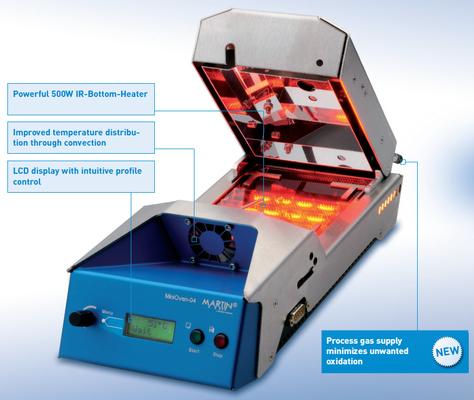
Desktop Reflow Oven For Reballing and Prebumping of SMD Components The new MiniOven-04 is perfectly suitable for a wide range of applications, from small QFNs to very large BGAs. This is due to our extensive selection of stencils and masks for almos
Used SMT Equipment | Pick and Place/Feeders
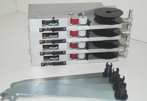
8mm, 12mm, 16mm, 24mm, 32mm, 44mm IQ ( Intelligent ) Surface Mount Tape Feeders and tape feeder reel arms for QUAD Q series and C series pick and place machines. These are the newer 8 pin, deep pocket, feeders and they will work on the newer intellig
Used SMT Equipment | Pick and Place/Feeders
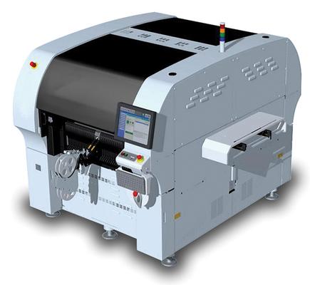
60,000cph with a large component range of 0201 to 30mmx30mm. Flexible, high-speed productivity for medium volume environments. A powerful line booster solution or high-performance small part placer. Dual-beam, dual-drive overhead gantry system
Technical Library | 2015-12-02 18:32:50.0
(Thermal Compression with Non-Conductive Paste Underfill) Method.The companies writing this paper have jointly developed Copper (Cu) Pillar micro-bump and TCNCP(Thermal Compression with Non-Conductive Paste) technology over the last two+ years. The Cu Pillar micro-bump and TCNCP is one of the platform technologies, which is essentially required for 2.5D/3D chip stacking as well as cost effective SFF (small form factor) package enablement.Although the baseline packaging process methodology for a normal pad pitch (i.e. inline 50μm) within smaller chip size (i.e. 100 mm2) has been established and are in use for HVM production, there are several challenges to be addressed for further development for commercialization of finer bump pitch with larger die (i.e. ≤50μm tri-tier bond pad with the die larger than 400mm2).This paper will address the key challenges of each field, such as the Cu trace design on a substrate for robust micro-joint reliability, TCNCP technology, and substrate technology (i.e. structure, surface finish). Technical recommendations based on the lessons learned from a series of process experimentation will be provided, as well. Finally, this technology has been used for the successful launching of the company FPGA products with SFF packaging technology.
Technical Library | 2018-04-05 10:40:43.0
The miniaturization of microchips is always driving force for revolution and innovation in the electronic industry. When the pitch of bumps is getting smaller and smaller the ball size has to be gradually reduced. However, the reliability of smaller ball size is getting weaker and weaker, so some traditional methods such as capillary underfilling, corner bonding and edge bonding process have been being implemented in board level assembly process to enhance drop and thermal cycling performance. These traditional processes have been increasingly considered to be bottleneck for further miniaturization because the completion of these processes demands more space. So the interest of eliminating these processes has been increased. To meet this demand, YINCAE has developed solder joint encapsulant adhesives for ball bumping applications to enhance solder joint strength resulting in improving drop and thermal cycling performance to eliminate underfilling, edge bonding or corner bonding process in the board level assembly process. In this paper we will discuss the ball bumping process, the reliability such as strength of solder joints, drop test performance and thermal cycling performance.
Technical Library | 2007-06-27 15:43:06.0
Traditionally most flip chips were designed with large bumps on a coarse pitch. However, as the trend towards smaller, more compact assemblies continues the sizes of semiconductor packages are forced to stay in line. New designs are incorporating smaller bump diameters on increasingly aggressive pitches, and in many cases decreasing the total IO count. With fewer and smaller bumps to distribute the load of the placement force it is becoming increasingly vital for equipment manufacturers to meet the challenge in offering low force placement solutions. One such solution will be presented in the following discussion. Also presented will be ways to minimize the initial impact spike that flip chips experience upon placement.
Technical Library | 2015-09-23 22:08:32.0
A molded interconnect device (MID) is an injection molded thermoplastic substrate which incorporates a conductive circuit pattern and integrates both mechanical and electrical functions. (...) Flip chip bonding of bare die on MID can be employed to fully utilize MID’s advantage in device miniaturization. Compared to the traditional soldering process, thermo-compression bonding with gold stud bumps provides a clear advantage in its fine pitch capability. However, challenges also exist. Few studies have been made on thermocompression bonding on MID substrate, accordingly little information is available on process optimization, material compatibility and bonding reliability. Unlike solder reflow, there is no solder involved and no “self-alignment,” therefore the thermo-compression bonding process is significantly more dependent on the capability of the machine for chip assembly alignment.
Industry Directory | Consultant / Service Provider / Manufacturer
HEPCO, Inc. is the world's leading manufacturer of Component Lead Prep, BGA Reballing, and RoHS/WEEE & Lead-Free Testing Equipment.


