Industry News | 2010-06-30 12:22:22.0
Two IEEE standards on setting criteria for environmentally preferable electronic equipment will soon go to ballot: 1680.2 Draft Standard for Environmental Assessment of Imaging Equipment and 1680.3 Draft Standard for the Environmental Assessment of Televisions...

The PCB Footprint Expert is a powerful CAD library development tool powered by our own proprietary CAD LEAP Technology (Libraries Enhanced with Automated Preferences). It is packed with very powerful advanced library management features that cuts foo

The PCB Footprint Expert is a powerful CAD library development tool powered by our own proprietary CAD LEAP Technology (Libraries Enhanced with Automated Preferences). It is packed with very powerful advanced library management features that cuts foo
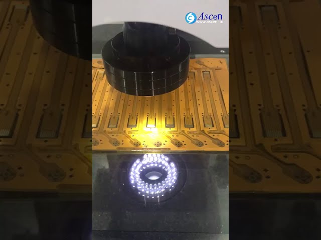
https://www.ascen.ltd/Products/PCB_board_assembly_system/vision_measurin/507.html Vision Measuring Machine and image measuring instrument can be used for dimensional accuracy measurement of various molds, aircraft, automobile, mobile phone, computer,
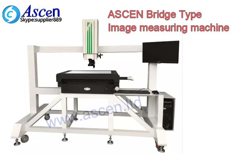
Bridge Type Image measuring machine Instrument features: 1.Adopt high precision grantie structure, never deformation,high stablility and high end good looking . 2.Adopted high-precision optical granite structure ,high resolution color charge-c
Industry News | 2020-04-29 07:26:56.0
Since the 'normal life' as we know it, has been interrupted by Coronavirus pandemic, we have noted the following;
Industry News | 2009-04-21 13:50:36.0
FREMONT, CA � April 2009 � Alta Manufacturing, a leading contract manufacturer specializing in NPI to pilot production of complex PCBs, announces that it has formed a strategic alliance with Alta Via Technologies in an exclusive agreement to develop and implement an innovative technology roadmap that advances the state-of-the-art in the Layout, Fabrication, and Assembly of complex printed circuit boards.
Technical Library | 2021-07-20 20:02:29.0
During the manufacturing of printed circuit boards (PCBs) for a Flight Project, it was found that a European manufacturer was building its boards to a European standard that had no requirement for copper wrap on the vias. The amount of copper wrap that was measured on coupons from the panel containing the boards of interest was less than the amount specified in IPC-6012 Rev B, Class 3. To help determine the reliability and usability of the boards, three sets of tests and a simulation were run. The test results, along with results of simulation and destructive physical analysis, are presented in this paper. The first experiment involved subjecting coupons from the panels supplied by the European manufacturer to thermal cycling. After 17 000 cycles, the test was stopped with no failures. A second set of accelerated tests involved comparing the thermal fatigue life of test samples made from FR4 and polyimide with varying amounts of copper wrap. Again, the testing did not reveal any failures. The third test involved using interconnect stress test coupons with through-hole vias and blind vias that were subjected to elevated temperatures to accelerate fatigue failures. While there were failures, as expected, the failures were at barrel cracks. In addition to the experiments, this paper also discusses the results of finite-element analysis using simulation software that was used to model plated-through holes under thermal stress using a steady-state analysis, also showing the main failure mode was barrel cracking. The tests show that although copper wrap was sought as a better alternative to butt joints between barrel plating and copper foil layers, manufacturability remains challenging and attempts to meet the requirements often result in features that reduce the reliability of the boards. Experimental and simulation work discussed in this paper indicate that the standard requirements for copper wrap are not contributing to the overall board reliability, although it should be added that a design with a butt joint is going to be a higher risk than a reduced copper wrap design. The study further shows that procurement requirements for wrap plating thickness from Class 3 to Class 2 would pose little risk to reliability (minimum 5 μm/0.197 mil for all via types).Experimental results corroborated by modeling indicate that the stress maxima are internal to the barrels rather than at the wrap location. In fact, the existence of Cu wrap was determined to have no appreciable effect on reliability.
Industry News | 2010-10-20 23:29:54.0
Viasystems Group, Inc. and Faraday Technology, Inc. are collaborating on demonstration of the FARADAYIC(R) ElectroCell technology for the manufacture of printed circuit boards (PCBs) with high-density interconnect features and at high plating rates for improved productivity.

COT specializes in high quality SMT nozzles and consumables for pick and place machines. We provide special engineering design service of custom nozzles for those unique and odd components.
2481 Hilton Drive
Gainesville, GA USA
Phone: (770) 538-0411


