Industry News | 2019-11-05 22:17:26.0
Plated half holes(castellated holes)are holes that made off the edge of the boards plated with copper using a specialized process. It is predominantly used for board-on-board connections, mostly where two printed circuit boards with different technologies are combined. Through connecting the PCBs together directly, the whole system is considerably thinner than a comparable connection with multi-pin connectors.The plated edges are also useful in producing mini PCB modules.
Industry News | 2016-01-06 11:10:25.0
Ucamco published revision 2016.01 of the Gerber Format Specification. This revision adds new attributes for castellated holes (or PTH on the board edge) and for tooling and break-out holes.
Industry Directory | Consultant / Service Provider / Manufacturer
Providing production and prototype, SEC offers advanced technologies like LED thermal management, heavy copper, PTFE for RFMW, open and internal cavities and blind and buried vias that are certified to a diverse set of industries.
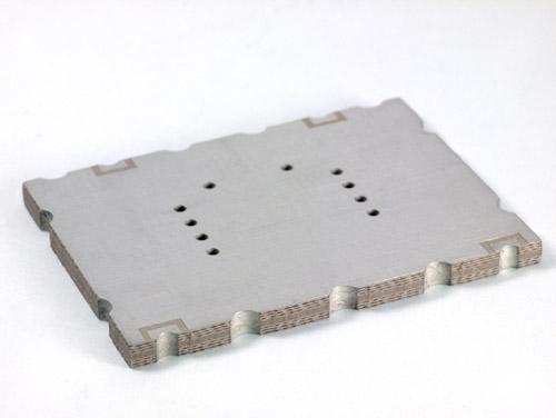
This multilayer, high-frequency coupler, shown above, is used within a communications application for the telecom industry. Multilayer High Frequency Coupler Specifications: Product Description This Multi-Layer High-Frequency Coupler is used with
Industry Directory | Manufacturer
PCBCart, a highly skilled PCB Fab, Parts Sourcing & Assembly services provider for global companies, fabricates 23k+ different PCB designs each year, and are committed on the quality & performance of every circuit board it printed
Training Courses | | | PCB Assembly Courses
The PCB assembly courses provide knowledge of different processes and equipment used in TH and SMT assembly of printed circuit boards.
At Barry: custom requests are common and welcome. We enjoy the challange. Extensive capabilities, wide material selection and state-of-the-art equiptment (including in-house plating and machining) ensure we can deliver a component fitting your exact
Industry News | 2013-11-14 18:35:01.0
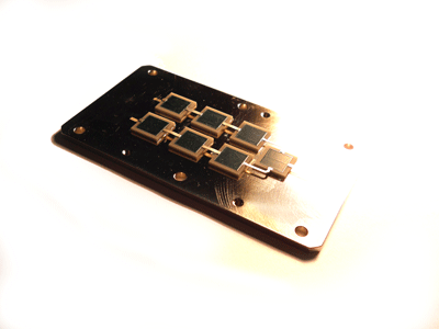
Barry Industries introduces their line of hermetically sealable HTCC Quad-Flat-No-Lead (QFN) packages with air cavity for high frequency applications. These QFN packages are available in six (6) sizes from 3mm to 8mm with standard JEDEC MO-220 footprints.
Industry News | 2015-03-16 06:51:04.0
Void Formation in Solder Joints – Causes & Cures Webinar Monday 18th May 2.30pm GMT Voiding in solder joints is not new we have experienced cavities in solder joints during the introduction of through hole, surface mount and more recently area array technology. In many cases we never knew we have had voids till the introduction of x-ray inspection.
New Equipment | Assembly Services
TW-HDI PCB 0245 Price: Get Latest Price Minimum Order Quantity: 10 Unit/Units other Port: HK Packaging Details: blister and package Delivery Time: 1 week Payment Terms: L/C,D/P,T/T,Western Union Supply Ability: 5000000 Unit/Units per Year o
.jpg)


