
MLT provides rigid and flexible circuit laser services including laser routing (excising), cavity skiving, coverlay/coverfilm routing, microvia drilling, ZIF Contours, Kapton window skives, depaneling, and marking. With 20 years experience, MLT has

For assembling connectors used in aerospace, medical, and other high-reliability applications. Light fibers driven by super-bright LED lamps individually illuminate target cavities in the connector being assembled. • Light-directed guided assembly
Technical Library | 2023-07-25 16:25:56.0
This paper address two significant applications of stencils in advance packaging field: 1. Ultra-Thin stencils for miniature component (0201m) assembly; 2. Deep Cavity stencils for embedded (open cavity) packaging. As the world of electronics continues to evolve with focus on smaller, lighter, faster, and feature-enhanced high- performing electronic products, so are the requirement for complex stencils to assemble such components. These stencil thicknesses start from less than 25um with apertures as small as 60um (or less). Step stencils are used when varying stencil thicknesses are required to print into cavities or on elevated surfaces or to provide relief for certain features on a board. In the early days of SMT assembly, step stencils were used to reduce the stencil thickness for 25 mil pitch leaded device apertures. Thick metal stencils that have both relief-etch pockets and reservoir step pockets are very useful for paste reservoir printing. Electroform Step-Up Stencils for ceramic BGA's and RF Shields are a good solution to achieve additional solder paste height on the pads of these components as well as providing exceptional paste transfer for smaller components like uBGAs and 0201s. As the components are getting smaller, for example 0201m, or as the available real estate for component placement on a board is getting smaller – finer is the aperture size and the pitch on the stencils. Aggressive distances from step wall to aperture are also required. Ultra-thin stencils with thicknesses in the order of 15um-40um with steps of 15um are used to obtain desired print volumes. Stencils with thickness to this order can be potential tools even to print for RDLs in the package.

More Product Information: EN: http://www.essemtec.com/en/products/dispensing/tarantula/ DE: http://www.essemtec.com/produkte/smt-dosieren/tarantula/ Introducing - The Tarantula - State of the art technology, easily integrated in any line. Wide range
Used SMT Equipment | In-Circuit Testers
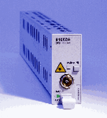
The Agilent-Hp 8166xA Distributed Feedback Laser Sources are part of the Agilent Lightwave Solution Platform, and best suited for amplifier test and DWDM system test applications. Agilent covers the C- and L-Band with its family of Distributed Feedba
Used SMT Equipment | In-Circuit Testers
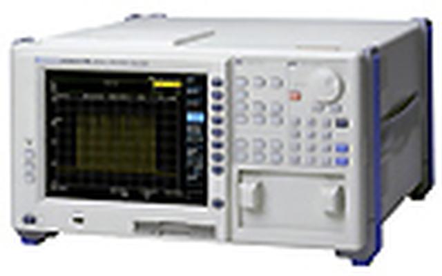
Ando AQ6315E Optical Spectrum Analyzer The AQ6315E optical spectrum analyzer (OSA) is an improved version of the well known Ando AQ6315A. This OSA can do spectrally resolved intensity measurements in the range of 350 to 1750 nm with a wavelengt

Used SMT Equipment | General Purpose Test & Measurement
We ship worldwide. Please feel free to contact us if you need further information. Agilent 81949A Compact Tunable Laser Source, 1520nm to 1630nm Key perfomance values High optical output power: +13 dBm Wide tuning range: 1520nm-1630nm Absolute
Used SMT Equipment | General Purpose Test & Measurement
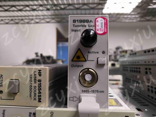
Key Features & Specifications High optical output power: +13 dBm Wide tuning range: 1465nm-1575nm Built-in wavemeter for excellent accuracy: +/-20pm Built-in coherence control Stimulated Brillioun scattering suppression Description Keys

New Equipment | Fabrication Services
RF & Microwave PCB's ACI is a leader in providing complex RF/Microwave PCB’s covering a wide spectrum of product types including Defense/Aerospace, Medical Device, Imaging, and Telecommunications Equipment. ACI supports a wide range of frequency ban

Waffletechnology� cleaning cards incorporate flexible, raised platforms on their top and bottom surfaces. These cleaning platforms are essentially spring-loaded, significantly increasing the pressure applied to the internal components as the card pas


