Applied Ceramics is a fabricator of custom-made ceramics, quartz, silicon and sapphire spare parts designed for the semiconductor industry.
Industry Directory | Manufacturer
Pantronix offers a large array of standard and customized semiconductor and photonic packaging. These include: Hi-Rel & Custom Ceramic Packaging, Memory Modules, Optical Devices, Plastic Packaging, and Photonic Packaging.
New Equipment | Rework & Repair Services
BGA Reballing and Solder Bumping for all types of SMD's Lead, Lead Free and Solder Alloy Conversion. Package types include but are not limited to: PBGA (Plastic Ball Grid Array) TBGA (Tape Ball Grid Array) uBGA (Micro BGA) CCGA (Ceramic Colum
New Equipment | Education/Training
This course is designed for students that require the hands-on skill and knowledge to reliably remove and install many types of the most complex BGA components. Students are taught methods for safe and reliable BGA component rework using a top of the
Electronics Forum | Wed Aug 20 10:27:25 EDT 2003 | Dan Gosselin
Do any of you guys have a list of parts that cannot survive hanging upside down during reflow soldering. As our board designs become increasingly dense and higher speed, we need to use all available pcb real estate. This means locating parts we hi
Electronics Forum | Mon Feb 25 21:09:48 EST 2002 | davef
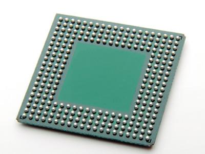
You are correct about a TCE [CTE] mismatch issues in ceramic packages. The coefficient of thermal expansion [ppm/�C] of major ceramic package elements are: * Silicon - 3 * Standard 92% alumina ceramic � 6.5 * FR4 board � 18-20 Several points are: *

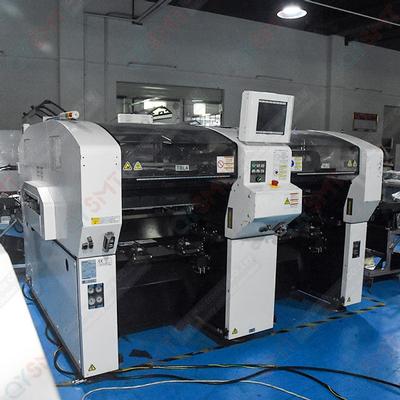
Used SMT Equipment | Pick and Place/Feeders
Panasonic CM602-L high-speed module placement machine, CM602-L placement machine not only follows the original module of Panasonic CM402, but also adds 12 nozzle high-speed head and direct suction tray as needed. The function of the original 8 nozzle
Used SMT Equipment | Pick and Place/Feeders
Panasonic CM602-L high-speed module placement machine, CM602-L placement machine not only follows the original module of Panasonic CM402, but also adds 12 nozzle high-speed head and direct suction tray as needed. The function of the original 8 nozzle
Industry News | 2003-04-15 08:57:18.0
First Implementation of the Package Platform Delivers 50-percent Cost, 60-percent Height, and 75-percent Area Reductions over Conventional RF Module Technologies
Industry News | 2003-04-18 08:31:57.0
Unichem to enhance its support and service for North American dry film photoresist and soldermask lamination equipment customers.
Parts & Supplies | Assembly Accessories
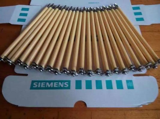
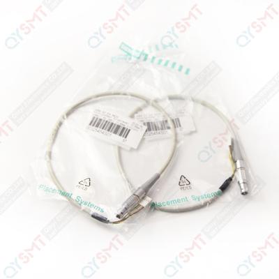
Detailed Product Description Brand: Siemens Country: China Shenzhen Condition: Made In China Model: 00318290-03/00351844-01 Use: For Siemens Siplace Name: Head Shaft Siemens F5 F5HM IC Head Shaft Ceramic 00318290-03 / 00351844-01 Detail Info
Parts & Supplies | Pick and Place/Feeders
00384300-01 SIPLACE Maintenance Manager V1.0, consisting of SIPLACE Maintenance Manager and Maintenance Plan Builder, is an additional software package to SIPLACE Explorer. Both software modules are designed for visualization, observation, analyses a
Technical Library | 2006-11-14 12:48:31.0
Content: 1. Bridge from Commercial Reliability 2. Existing PBGA use in Aerospace & Military 3. Drivers: Plastic versus Ceramic Package Weight 4. Attributes of PTFE and Thin Core FC Packages 5. Flip Chip Package Reliability 6. Flip Chip Package
Technical Library | 2017-06-15 00:44:19.0
Ceramics packages are being used in the electronics industry to operate the devices in harsh environments. In this paper we report a study on acoustic imaging technology for nondestructively inspecting underfill layers connecting organic interposers sandwiched between two ceramics substrates.First, we inspected the samples with transmission mode of scanning acoustic tomography (SAT) system, an inspection routine usually employed in assembly lines because of its simpler interpretation criteria: flawed region blocks the acoustic wave and appears darker. In this multilayer sample, this approach does not offer the crucial information at which layer of underfill has flaws. To resolve this issue, we use C-Mode Scanning in reflection mode to image layer by layer utilizing ultrasound frequencies from 15MHz to 120MHz. Although the sample is thick and contains at least 5 internal material interfaces, we are able to identify defective underfill layer interfaces.
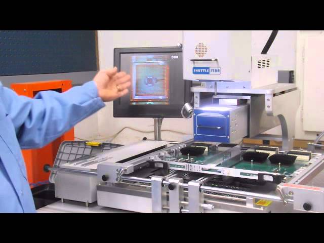
Dennis Odonnell , Vice President of Precision PCB Services, Inc., Oroville CA Explains How to Evaluate a BGA Rework Station ! #BGA Rework Stations http://www.pcb-repair.com/bga-rework-station/
Dennis Odonnell , Vice President of Precision PCB Services, Inc., Oroville CA Explains How to Evaluate a BGA Rework Station ! #BGA Rework Stations http://www.pcb-repair.com/bga-rework-station/
Training Courses | | | PCB Rework and Hand Soldering Courses
The PCB rework and hand soldering courses courses cover techniques of rework and repair of PCBs, BGAs and other electronics assemblies, and teach fundamentals of soldering of electronics assemblies.
Training Courses | | | PCB Rework and Hand Soldering Courses
The PCB rework and hand soldering courses courses cover techniques of rework and repair of PCBs, BGAs and other electronics assemblies, and teach fundamentals of soldering of electronics assemblies.
Events Calendar | Tue Sep 08 00:00:00 EDT 2020 - Tue Sep 08 00:00:00 EDT 2020 | ,
Post – Moore's Law Electronics: From Now until Quantum Computing
Events Calendar | Tue Feb 19 00:00:00 EST 2019 - Tue Feb 19 00:00:00 EST 2019 | ,
Webinar: BGA Reballing - Theory and Hands On
Career Center | Space Coast, Florida USA | Engineering,Research and Development
Board Level Assembly BGA Expert! We are in need of an Electronic Packaging or Advanced Manufacturing Engineer to work with the Advanced Manufacturing Technology Group of a major Florida based Communications company. Support IR&D and Program activit
Career Center | Melbourne, Florida USA | Engineering
Advanced Manufacturing Technology Position Description Job Description: AMT Engineer � Level 4 Support IR&D and Program activities Division wide working on the development, qualification, and implementation of electronic packaging technologies, wi
Career Center | seoul, South Korea | Engineering
I have 4 year process engineering in Motorola and 7 years service experience in Assemblen . 2 years in Mirtec AOI as service manager .
Career Center | ORLANDO, Florida USA | Engineering,Maintenance,Production,Technical Support
Manufacturing tech/eng for a contract manufacture for 10+ years. Been working in the SMT industry for a total of 20yrs. Have done everything from operator to process work. Most familiar with Assembleon, MPM, DEK, BTU,Electrovert, SLIM-KIC, SUPER-MOLE
SMTnet Express, June 15, 2017, Subscribers: 30,470, Companies: 10,610, Users: 23,373 Nondestructive Inspection of Underfill Layers Stacked up in Ceramics-Organics-Ceramics Packages with Scanning Acoustic Tomography (SAT) Flex International
| http://www.thebranfordgroup.com/dnn3/Auctions/RecentAuctions.aspx
Jabil Marcianise / Wuhan [Online] SOLD - Auction Closed on 8/12/2021 (2) Surplus Packages of Test & Measurement Equipment Oscilloscopes, Multimeters, Network Testers & More! Marcianise, Italy: (1,000+) Pieces of ETM Equipment Wuhan, China: (20+) Pieces


