Our company provides the Freeware (up to 250 pins) program for PCB Hobbyists and Professionals. It includes Schematics, PCB Layout, Autorouter, Component Editorand and libraries. With DipTrace you can produce the PCB's using milling method.
Industry Directory | Consultant / Service Provider / Manufacturer / Other
Global provider of Legacy PCB Re-Engineering Systems & Process Control Tools since 1990.
Used SMT Equipment | Pick and Place/Feeders
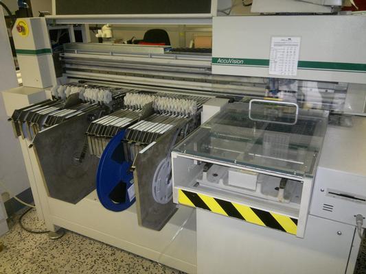
PicK & Place CONTACT 3AV used but in very good condition , 220V with two heads each with 2 nozzles. Accompanied by a hundred feeder of different sizes, of which 65 in good condition and 40 are in need of a tune-up, plus four vibrated. Optical Posit

Used SMT Equipment | AOI / Automated Optical Inspection
Mirtec MV-2HTL Desktop Automated Optical Inspection Machine (2003) Brand: Mirtec Model: MV-2HTL Type: Automated optical inspection machine Serial #: 01031226-0227 Year: 2003 Voltage: 100V-240V /4.4A /50-60Hz Standard Features: Pentium&trad
Used SMT Equipment | AOI / Automated Optical Inspection
CyberOptics FLEX ULTRA (2010) High Resolution Automated Optical Inspection Machine Brand: CyberOptics Model: FLEX ULTRA Year: 2010 Serial: 70246 Type: Automated Optical Inspection Machine Product details: The new Flex Ultra HR is the latest
Career Center | Longmont, Colorado USA | Production
Small high mix low volume shop looking for Machine Operator. This position will be responsible for the set-up and operation of Dymaxion (Primary) and Samsung placement machines. Knowledge of machine operational theory a big plus. Company will train
Supply chain management expert, Zurvahn is an Electronic Manufacturing Service provider for mid- to low-volume products to Original Equipment Manufacturers worldwide.
Training Courses | | | PCB Design Courses
The PCB design courses teach students the process, techniques and tools needed to design layout of printed circuit boards.
Used SMT Equipment | Pick and Place/Feeders
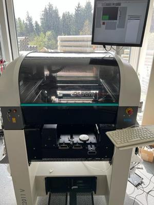
This item has been used by our production lab for small scale production since 2015 and is in very good condition. Item includes the following accessories: FLX2011 Highly flexible Pick and Place system with optical laser ce
Career Center | Rancho Santa Margarita, CA USA | Engineering
Viking Components, one of the world's largest and fastest-growing manufacturers of component technology, designs and manufactures computer memory, modems and flash memory products for the retail, reseller and OEM markets has an immediate opening for


winsouce.jpg)