Industry Directory | Manufacturer
Twisted Traces, a US-based leader in the printed circuit board manufacturing industry, offers unmatched benefits on three fronts: quality, cost, and on-time delivery.
Industry Directory | Distributor / Equipment Dealer / Broker / Auctions
Electronic Component Distribution has a wide-ranging inventory of electronic items. We are Board Level Components and Electronic Part Types supplier in the USA.
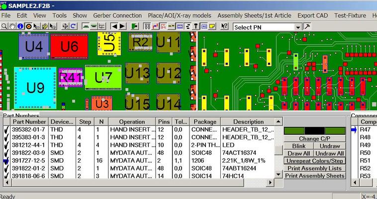
ProntoPLACE used by electronics manufacturers will quickly program your surface mount SMT and thru-hole assembly equipment. In minutes Unisoft ProntoPLACE software translates CAD or Gerber and Bill of Materials (BOM) files into real reference desig
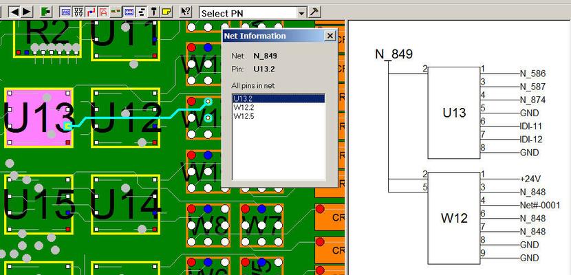
ProntoTEST-FIXTURE used by electronics manufacturers will accurately setup your Automatic Test Equipment (ATE), Flying Probe and design your "bed of nails" test fixturing. In minutes Unisoft ProntoTEST-FIXTURE software translates CAD and Bill of Ma
Electronics Forum | Thu Feb 04 06:50:35 EST 1999 | Greg Flynn
What allowances are people using out there for components off-pad, we currently use 50% of lead width without breaking trace/component clearances but we have a customer demanding 25% allowance ?
Electronics Forum | Thu Feb 04 09:09:11 EST 1999 | Peet
| What allowances are people using out there for components off-pad, we currently use 50% of lead width without breaking trace/component clearances but we have a customer demanding 25% allowance ? | We use 50% for civile application, and 25% for mil
Used SMT Equipment | In-Circuit Testers
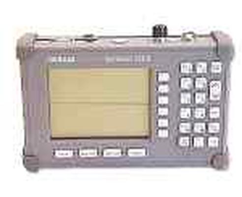
3300MHz Cable Antenna Analyzer SiteMaster The Anritsu S331B SiteMaster, with frequency coverage of 25 MHz to 3300 MHz, is ideally suited for users who work in VHF, broadcasting, paging, cellular, PCS/GSM and ISM and WLL frequency bands. Both S331B
Used SMT Equipment | Pick and Place/Feeders
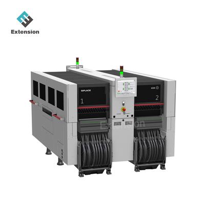
Make: ASMModel:ASM SIPLACE CA Details:1. High-Speed Placement CapabilitySMT component placement speed up to 76,000 components per hour (Cph).Flip chip placement from wafer up to 40,000 Cph.Die attach placement from wafer up to 50,000 Cph. 2. Placemen
Industry News | 2018-09-06 12:12:07.0
GPD Global offers the ideal tabletop robots (Catalina Series) for precision dispensing.
Industry News | 2018-02-12 12:28:00.0
GPD Global introduces its NEW full-featured benchtop dispensing robot system: Catalina. A benchtop system does not mean "no features". This compact and efficient semi-auto dispense robot provides you with numerous standard features: automatic vision, laser surface sensing, and automatic nozzle alignment and calibration.
.jpg)
Parts & Supplies | SMT Equipment
00378485-02 SMD TAPE CONNECTOR 16mm ESD 00378511-02 Protective Tape Scotch 2104c, 12mm wide 00378539-01 plus expenses 00378544-01 PLATE FOR DIP-MODUL 00378599-01 SOFTWARE SIPLACE STATION 408.01 Update 00378600-01 SOFTWARE SIPLACE STATION 408/1-4
Parts & Supplies | Circuit Board Assembly Products
Specifications 1.One-stop OEM pcb assembly service. 2.ROHS, SGS, UL certificated 3.Reasonable price 4.High Quality 5.Fast Delivery PCB Assembly&PCBA Service 1. Experienced components sourcing team specially for scarce parts 2.1 to 12 layers m
Technical Library | 2020-03-26 14:55:29.0
This paper introduces line confocal technology that was recently developed to characterize 3D features of various surface and material types at sub-micron resolution. It enables automatic microtopographic 3D imaging of challenging objects that are difficult or impossible to scan with traditional methods, such as machine vision or laser triangulation.Examples of well-suited applications for line confocal technology include glossy, mirror-like, transparent and multi-layered surfaces made of metals (connector pins, conductor traces, solder bumps etc.), polymers (adhesives, enclosures, coatings, etc.), ceramics (components, substrates, etc.) and glass (display panels, etc.). Line confocal sensors operate at high speed and can be used to scan fast-moving surfaces in real-time as well as stationary product samples in the laboratory. The operational principle of the line confocal method and its strengths and limitations are discussed.Three metrology applications for the technology in electronics product manufacturing are examined: 1. 3D imaging of etched PCBs for micro-etched copper surface roughness and cross-sectional profile and width of etched traces/pads. 2. Thickness, width and surface roughness measurement of conductive ink features and substrates in printed electronics applications. 3. 3D imaging of adhesive dots and lines for shape, dimensions and volume in PCB and product assembly applications.
Technical Library | 2023-11-06 17:08:44.0
A new process has been developed for RF shielding on compact electronic communications devices using automated solder paste dispensing. The process is known as Shield Edge Interconnect (SEI). SEI designs enable parts to be processed though underfill before placing of the RF shield and allows more complete use of valuable PCB real estate to achieve reduced form factor requirements and/or for added components on products such as smartphones and tablets. The reduced form factor creates challenges for the assembly of those devices. This process, enabled by Speedline dispensing technology, relies on extremely accurate dispensing of solder paste on copper traces located along the outer edge of the PCB. The result is a robust process solution for SEI in which proprietary closed loop dispenser, pump, vision, and software technologies enable a high volume manufacturing (HVM) process.

www.unisoft-cim.com/pcbplace.htm - The ProntoPLACE module from Unisoft is used by electronics manufacturers to generate the necessary programs for automatic PCB assembly machines in minutes. ProntoPLACE programs most popular surface mount (SMT) place

www.unisoft-cim.com/pcbtest.htm - In minutes the Unisoft ProntoTEST-FIXTURE software translates CAD & BOM files into real reference designators, netlists, X/Y component pin geometries, values, tolerances, part numbers, etc. This data is used by Test
Training Courses | | | IPC-7711/7721 Specialist (CIS) Recert.
The Certified IPC-7711/7721 Specialist (CIS) recertification courses are intended for those individuals who were previously certified as IPC-7711/7721 Specialist.
Training Courses | | | IPC-7711/7721 Trainer (CIT)
The Certified IPC-7711/7721 Trainer (CIT) courses recognize individuals as qualified trainers in the area of rework and repair of printed boards and electronic assemblies and prepares them to deliver Certified IPC-7711/7721 (CIS) training.
Career Center | Madison, Alabama USA | Engineering,Production
Performs electronic assembly functions on an as needed basis. Performs rework/replacement/placement operations on BGAs using various rework systems without doing damage to the assemblies. Performs X-ray inspection of BGAs using CRX-2000 real time
Career Center | Fremont, California USA | Engineering
Interprets electrical design requirements and uses Allegro design tool to create original PCB layouts, detailed fab drawings, schematics, and other design files. Work with HW design engineer to make sure PCB layout meet PCB design requirements.
Career Center | seoul, South Korea | Engineering
I have 4 year process engineering in Motorola and 7 years service experience in Assemblen . 2 years in Mirtec AOI as service manager .
New Methods of Testing PCB Traces Capacity and Fusing New Methods of Testing PCB Traces Capacity and Fusing by: Norocel Codreanu, Radu Bunea, Paul Svasta; "Politehnica" University of Bucharest, Center for Technological Electronics
PCB Libraries, Inc. | https://www.pcblibraries.com/Forum/pqfn-pson-footprint-name_topic305.html
“ The minimum board edge to any feature - component, via, trace, copper pour is 40 mils (1.0 mm)”. I have a hard time with IPC spec’s and where to find out things like that. I have been using .040 for planes and .020 for traces
Imagineering, Inc. | https://www.pcbnet.com/capabilities/fabrication/tolerances/
″ over finished hole size for vias and + 0.012″ over finished hole size for component holes. This means the annular ring (radius of the pad) should be at least


