Industry News | 2019-04-15 06:54:35.0
Engineered Material Systems exhibit in Hall C1, booth 354 at the Intersolar Europa Solar Power Expo, scheduled to take place May 15-17, 2019 in Munich, Germany. Company representatives will show next-generation low-cost electrically conductive adhesives for stringing, shingling and back contact applications in crystalline silicon and heterojunction solar modules.
New Equipment | Cleaning Agents
220°F~104°C Boiling Point 280°F~138°C Water Soluble Complete VOC, @10% 90.0 g/L Typical Processes: Application Spray
New Equipment | Cleaning Agents
220°F/104°C Boiling Point 240°F/115°C Water Soluble Complete VOC, @10% 88.9 g/L Typical Processes: Application In-Line
New Equipment | Cleaning Agents
200°F~93°C Boiling Point: 292°F~144°C Water Soluble: Partially miscible VOC, @ 10%: 88.45 g/L Typical Processes Application: Spray-in-Air / Select Ultrasonic Stencil Cleaners Concentration: 25% Temperature: Ambient to Rinse: Optional Dry

6 hours Thin Film Set Time (.001" @ 25°C) >12 hours Total % NV Solids 100% Hegman Gauge Volume Resi
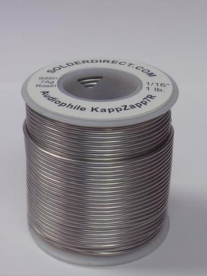
New Equipment | Solder Materials
KappZapp7R Rosin-cored Solder has rapidly become the audio industry standard for electrical / electronic Copper applications. The 7% Silver solder creates extremely clean conductive joints with high strength, ductility and corrosion resistance. The c
Career Center | South Plainfield, New Jersey USA | Engineering,Research and Development
MacDermid Alpha Electronics Solutions, a world leader in the development, manufacturing, and sales of innovative materials used in the assembly electronics, industrial joining and Photo Voltaic market places, is seeking a Scale-Up Technician/Chemist&
Technical Library | 2023-03-16 18:51:43.0
Conductive anodic filament (CAF) formation was first reported in 1976.1 This electrochemical failure mode of electronic substrates involves the growth of a copper containing filament subsurface along the epoxy-glass interface, from anode to cathode. Despite the projected lifetime reduction due to CAF, field failures were not identified in the 1980s. Recently, however, field failures of critical equipment have been reported.2 A thorough understanding of the nature of CAF is needed in order to prevent this catastrophic failure from affecting electronic assemblies in the future. Such an understanding requires a comprehensive evaluation of the factors that enhance CAF formation. These factors can be grouped into two types: (1) internal variables and (2) external influences. Internal variables include the composition of the circuit board material, and the conductor metallization and configuration (i.e. via to via, via to surface conductor or surface conductors to surface conductors). External influences can be due to (1) production and (2) storage and use. During production, the flux or hot air solder leveling (HASL) fluid choice, number and severity of temperature cycles, and the method of cleaning may influence CAF resistance. During storage and use, the principal concern is moisture uptake resulting from the ambient humidity. This paper will report on the relationship between these various factors and the formation of CAF. Specifically, we will explore the influences of printed wiring board (PWB) substrate choice as well as the influence of the soldering flux and HASL fluid choices. Due to the ever-increasing circuit density of electronic assemblies, CAF field failures are expected to increase unless careful attention is focused on material and processing choices.
EP-1100 is a one-part adhesive epoxy designed for screen or stencil printing for component attachment, termination and other applications in: hybrid circuits membrane keypads other electromechanical assemblies EP-1100 exhibits excelle
Training Courses | | | IPC-7711/7721 Trainer (CIT)
The Certified IPC-7711/7721 Trainer (CIT) courses recognize individuals as qualified trainers in the area of rework and repair of printed boards and electronic assemblies and prepares them to deliver Certified IPC-7711/7721 (CIS) training.


