Industry News | 2016-05-09 21:47:59.0
Henkel Adhesive Technologies’ Electronics business today announced a new distribution partnership with plastic film and adhesives solutions provider, Tekra, A Division of EIS, Inc. Under the terms of the agreement, Tekra will deliver sales, technical consultation and post-sale service for Henkel’s full line of electronic ink materials in support of customers throughout North America.
Industry News | 2011-08-29 16:29:56.0
Engineered Conductive Materials debuts its DB-1580 Series Conductive Stringer Attach Adhesives for back contact applications in crystalline silicon solar modules.
Industry News | 2013-06-10 10:36:15.0
Conductive Compounds Inc. is now ISO 9001: 2008 Registered
Technical Library | 2020-03-26 14:55:29.0
This paper introduces line confocal technology that was recently developed to characterize 3D features of various surface and material types at sub-micron resolution. It enables automatic microtopographic 3D imaging of challenging objects that are difficult or impossible to scan with traditional methods, such as machine vision or laser triangulation.Examples of well-suited applications for line confocal technology include glossy, mirror-like, transparent and multi-layered surfaces made of metals (connector pins, conductor traces, solder bumps etc.), polymers (adhesives, enclosures, coatings, etc.), ceramics (components, substrates, etc.) and glass (display panels, etc.). Line confocal sensors operate at high speed and can be used to scan fast-moving surfaces in real-time as well as stationary product samples in the laboratory. The operational principle of the line confocal method and its strengths and limitations are discussed.Three metrology applications for the technology in electronics product manufacturing are examined: 1. 3D imaging of etched PCBs for micro-etched copper surface roughness and cross-sectional profile and width of etched traces/pads. 2. Thickness, width and surface roughness measurement of conductive ink features and substrates in printed electronics applications. 3. 3D imaging of adhesive dots and lines for shape, dimensions and volume in PCB and product assembly applications.
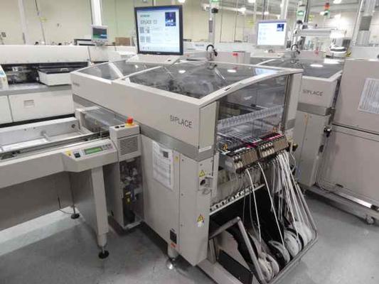
Used SMT Equipment | Pick and Place/Feeders
X-Line Assets will be conducting an online auction for surplus equipment to the ongoing operations of Artflex in Ottawa and Toronto. The auciton is slated for August 19-20. This machine will be included in the sale: Siemens Siplace CS Placement Sys
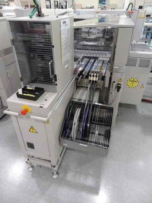
Used SMT Equipment | Pick and Place/Feeders
X-Line will be conducting an online auction for surplus equipment to the ongoing operations of Artflex in Ottawa and Toronto. The auciton is slated for August 19-20. This machine will be included in the sale: Siemens Siplace CF Placement System wit
Industry News | 2011-11-08 13:28:32.0
Engineered Conductive Materials introduces its DB-1588 low-cost conductive adhesive for back contact applications in crystalline silicon solar modules.

4 hours Thin Film Set Time (.001" @ 25°C) >12 hours Total % NV Solids 100% Hegman Gauge Volume Resi
Industry News | 2010-09-08 11:49:17.0
PCB Fabricator Installs MASS VHF 300 VS for Via Hole Filling Addressing the continuous demands pertaining to via hole filling, through holes and blind vias
Technical Library | 2018-01-11 10:48:48.0
Ink-jet printing is poised to impact the manufacturing of devices that are particularly attractive for flexible electronics, as more suitable and printable fluids become available. The addition of surfacants in the preparation of the inks usually results in additional process steps, potentially increasing cost, as well as material waste, where the surfactants also often have a negative impact on specific properties of the printed features, such as comprising electrical conductivity of metallic structures. (...)In this work, we have successfully formulated a suitable ink derived from a mixture of terpineolin cyclohexanone as a more environmentally friendly option for the exfoliation of bulk graphite, which we elaborate upon in more detail here.


