Industry News | 2012-11-20 17:30:48.0
On Dec 5-6, the Printed Electronics USA conference and exhibition in Santa Clara, CA, will feature "Manufacturing Street" - its first live, multi-technology, printed electronics demonstration. Being part of the exhibition, Manufacturing Street brings together organizations in the supply chain who will demonstrate a number of printing and process steps in interactive sessions throughout the event, printing functional inks.
Industry News | 2011-08-08 14:36:41.0
Engineered Conductive Materials, LLC will introduce its new line of conductive adhesives for back contact solar module applications in Hall A1, Stand B4 at the upcoming European Photovoltaic Solar Energy Conference and Exhibition (PVSEC), scheduled to take place September 5-8, 2011 at the CCH Congress Centre and International Fair in Hamburg, Germany.
Industry News | 2011-01-17 19:42:26.0
Engineered Conductive Materials, LLC, will showcase its DB-1541-X Series Conductive Stringer Attach Adhesives in Hall E7, Stand 655 at the upcoming SNEC International Photovoltaic Power Generation Conference & Exhibition, scheduled to take place February 22-24, 2011 at the Shanghai New International Expo Center in Shanghai, China.
Industry News | 2012-12-04 14:08:23.0
On Dec 5-6, attendees to the Printed Electronics USA conference and exhibition in Santa Clara, CA, will receive their own origami printed electronic device. One of the compelling benefits of printed electronics is that electronics can be used in completely new and innovative form factors.
Industry News | 2011-03-31 11:05:40.0
Engineered Conductive Materials, LLC will showcase its DB-1541-X Series Conductive Stringer Attach Adhesives in Hall A5, Stand 653 at the upcoming Intersolar Europe, scheduled to take place June 8-10, 2011 at the New Munich Trade Faire Centre in Munich, Germany.
Technical Library | 2021-11-03 16:52:47.0
This paper proposes the integration of pulsed photonic sintering into multi-material additive manufacturing processes in order to produce multifunctional components that would be nearly impossible to produce any other way. Pulsed photonic curing uses high power Xenon flash lamps to thermally fuse printed nanomaterials such as conductive metal inks. To determine the feasibility of the proposed integration, three different polymer additive manufacturing materials were exposed to typical flash curing conditions using a Novacentrix Pulseforge 3300 system. FTIR analysis revealed virtually no change in the polymer substrates, thus indicating that the curing energy did not damage the polymer. Next, copper traces were printed on the same substrate, dried, and photonically cured to establish the feasibility of thermally fusing copper metal on the polymer additive manufacturing substrates. Although drying defects were observed, electrical resistivity values ranging from 0.081 to 0.103 Ω/sq. indicated that high temperature and easily oxidized metals can be successfully printed and cured on several commonly used polymer additive manufacturing materials. These results indicate that pulsed photonic curing holds tremendous promise as an enabling technology for next generation multimaterial additive manufacturing processes.
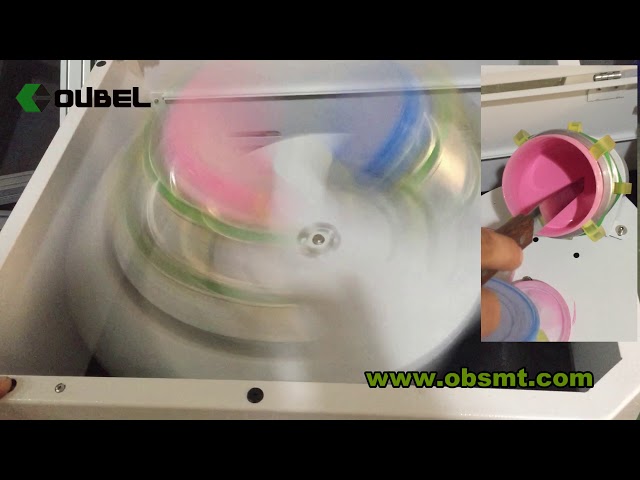
High speed mixer, centrifugal mixer 1200RPM More information, welcome to contact: Web: www.obsmt.com E:sales@obsmt.com T/ Wechat/ Whatsapp: +86 13926596436 Skype: xudan0525
Technical Library | 2018-10-18 15:41:45.0
One specific market space of interest to emerging printed electronics is In Mold Label (IML) technology. IML is used in many consumer products and white good applications. When combined with electronics, the In Mold Electronics (IME) adds compelling new product functionality. Many of these products have multi-dimensional features and therefore require thermoforming processes in order to prepare the labels before they are in-molded. While thermoforming is not a novel technique for IML, the addition of printed electronic functional traces is not well documented. There is little or no published work on printed circuit performance and design interactions in the thermoforming process that could inform improved IME product designs. A general full factorial Design of Experiments (DOE) was used to analyze the electrical performance of the conductive silver ink trace/polycarbonate substrate system. Variables of interest include trace width, height of draw, and radii of both top and bottom curvatures in the draw area. Thermoforming tooling inserts were fabricated for eight treatment combinations of these variables. Each sample has one control and two formed strips. Electrical measurements were taken of the printed traces on the polymer sheets pre- and post- forming with a custom fixture to evaluate the effect on resistance. The design parameters found to be significant were draw height and bottom radius, with increased draw and smaller bottom curvature radii both contributing to the circuits’ resistance degradation. Over the ranges evaluated, the top curvature radii had no effect on circuit resistance. Interactions were present, demonstrating that circuit and thermoforming design parameters need to be studied as a system. While significant insight impacting product development was captured further work will be executed to evaluate different ink and substrate material sets, process variables, and their role in IME.
Industry News | 2013-04-25 16:35:51.0
Engineered Material Systems will debut its new DB-1588-2 Low-Cost Conductive Adhesive for back contact applications in crystalline silicon solar modules in booth #W3-688 at the 2013 SNEC 7th International Photovoltaic Power Generation Conference & Exhibition, scheduled to take place May 14-16, 2013 at the Shanghai New International Expo Center in China.
Industry News | 2012-12-12 12:30:21.0
The second and final day of Printed Electronics USA in Santa Clara really illustrated how far the technologies had progressed and the huge variety of players in the field. The event, organized by IDTechEx, was the best and biggest edition of the series so far.


