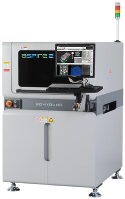
Koh Young Technology’s new product aSPIre 3D In-line Solder Paste Inspection System adds more value to your production. Keeping with high speed SMT lines, aSPIre system helps maximizing productivity and ensures no compromise is made between speed and
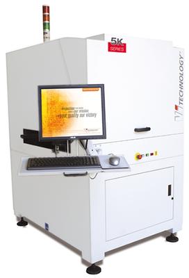
The large board solution The 5K Series offers flexibility for wider board applications and benefits from all the latest Vi TECHNOLOGY® innovations, including Selective 3D AOI technology for accurate tilt and coplanarity measurement of ICs, connector
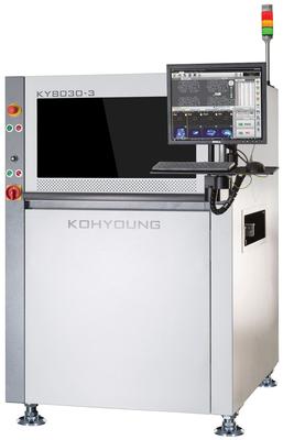
High-speed, High Performance 3D In-Line SPI with Dual Projection The new KY8030-3 delivers 3x faster inspection without compromising performance and accuracy. Using patented dual projection, the system eliminates the critical Shadow problem that al
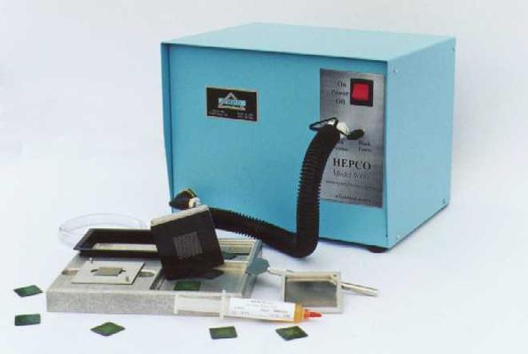
The Model 9000 operates using a self-contained vacuum system to secure the BGA component while transferring the desired pattern of solder sphere's in a full array. Alignment is achieved through precision pins and specific tooling for ease of use, re
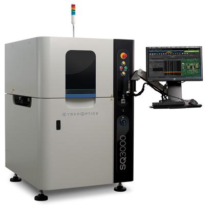
The Ultimate in Speed and Accuracy. SQ3000 3D Automated Optical Inspection (AOI) system maximizes ROI and line utilization with 3D multi-view sensors that enable fastest 3D inspection in the industry. SQ3000 incorporates Multi-Reflection Suppression
New Equipment | Soldering Robots
Constant-heated Bonding Machine Model No.: CHB312 Features: 1)Panasonic temperature controller ensures high accuracy heating control. 2)Omron dial knob timer enables easy operation and repeatability. 3)User can setup temperature, time and pres
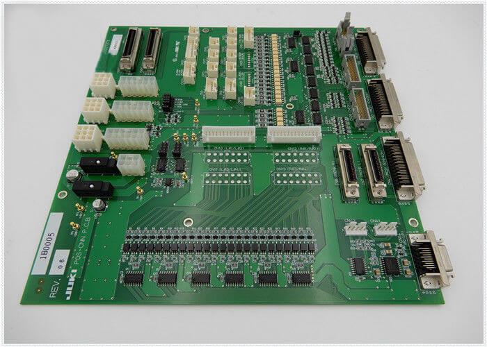
JUKI FX-1 FX-2 POSITION CONNECTION PCB ASM 40007372 JUKI FX-1 FX-2 POSITION CONNECTION PCB ASM 40007372 SMT Spare Parts JUKI Spare Parts Delivery time: 1-3 days Product description: JUKI FX-1 FX-2 POSITION CONNECTION PCB ASM 40007372 INQUI
Technical Library | 2014-03-06 19:04:07.0
Over the last few years, there has been an increase in the rate of Head-in-Pillow component soldering defects which interrupts the merger of the BGA/CSP component solder spheres with the molten solder paste during reflow. The issue has occurred across a broad segment of industries including consumer, telecom and military. There are many reasons for this issue such as warpage issues of the component or board, ball co-planarity issues for BGA/CSP components and non-wetting of the component based on contamination or excessive oxidation of the component coating. The issue has been found to occur not only on lead-free soldered assemblies where the increased soldering temperatures may give rise to increase component/board warpage but also on tin-lead soldered assemblies.
Technical Library | 2021-01-28 01:55:00.0
Printed circuit board surface finishes are a topic of constant discussion as environmental influences, such as the Restriction of Hazardous Substances (RoHS) Directive or technology challenges, such as flip chip and 01005 passive components, initiate technology changes. These factors drive the need for greater control of processing characteristics like coplanarity and solderability, which influence the selection of surface finishes and impact costs as well as process robustness and integrity. The ideal printed circuit board finish would have good solderability, long shelf life, ease of fabrication/processing, robust environmental performance and provide dual soldering/wirebonding capabilities; unfortunately no single industry surface finish possesses all of these traits. The selection of a printed circuit board surface finish is ultimately a series of compromises for a given application.
Technical Library | 2023-01-10 20:15:42.0
Over the past years there has been consistent growth in the use of electroless nickel / immersion gold (ENIG) as a final finish. The finish is now frequently being used for PBGA, CSP, QFP and COB and more recently gathered considerable interest as a low cost under-bump metallization for flip chip bumping application. One of the largest users for this finish has been the telecommunication industry, were millions of square meters of PCBs with ENIG have been successfully used. The nickel layer offers advantages such as multiple soldering cycles and hand reworks without copper dissolution being a factor. The nickel also acts as a reinforcement to improve through-hole and blind micro via thermal integrity. In addition the nickel layer offers advantages such as co-planarity, Al-wire bondability and the use as contact surface for keypads or contact switching. Especially those pads, which are not covered by solder need a protective coating in corrosive environment – such as high humidity or pollutant gas.


.png)

