Technical Library | 2008-03-13 13:02:50.0
Three full-field optical techniques, shadow moiré, fringe projection and digital image correlation (DIC), are used to measure temperature-dependent warpage for a PBGA package and a PCB component land site from room temperature to 250ºC. The results are qualitatively similar, but imaging resolution and noise properties create offsets between coplanarity values. The paper summarizes strengths and weaknesses for each technique.
Technical Library | 2017-08-31 13:43:48.0
Wire bonded packages using conventional copper leadframe have been used in industry for quite some time. The growth of portable and wireless products is driving the miniaturization of packages resulting in the development of many types of thin form factor packages and cost effective assembly processes. Proper optimization of wire bond parameters and machine settings are essential for good yields. Wire bond process can generate a variety of defects such as lifted bond, cracked metallization, poor intermetallic etc. NSOP – non-stick on pad is a defect in wire bonding which can affect front end assembly yields. In this condition, the imprint of the bond is left on the bond pad without the wire being attached. NSOP failures are costly as the entire device is rejected if there is one such failure on any bond pad. The paper presents some of the failure modes observed and the efforts to address NSOP reduction
Technical Library | 2023-08-04 15:38:36.0
The MicroLeadFrame® (MLF®)/Quad Flat No-Lead (QFN) packaging solution is extremely popular in the semiconductor industry. It is used in applications ranging from consumer electronics and communications to those requiring high reliability performance, such as the automotive industry. The wide acceptance of this packaging design is primarily due to its flexible form factors, size, scalability and thermal dissipation capabilities. The adaptation and acceptance of MLF/QFN packages in automotive high reliability applications has led to the development of materials and processes that have extended its capabilities to meet the performance and quality requirements. One of process developments that is enabling the success of the MLF/QFN within the automotive industry has been the innovation of side wettable flanks that provide the capability to inspect the package lead to printed circuit board (PCB) interfaces for reliable solder joints. Traditionally, through-board X-ray was the accepted method for detecting reliable solder joints for leadless packages. However, as PBC layer counts and routing complexities have increased, this method to detect well-formed solder fillets has proven ineffective and incapable of meeting the inspection requirements. To support increased reliability and more accurate inspection of the leadless package solder joints, processes to form side-wettable flanks have been developed. These processes enable the formation of solder fillets that are detectable using state-of-the-art automated optical inspection (AOI) equipment, providing increased throughput for the surface mount technology (SMT) processes and improved quality as well.
Technical Library | 2015-06-11 21:20:29.0
The use of bottom terminated components (BTC) has become widespread, specifically the use of Quad Flat No-lead (QFN) packages. The small outline and low height of this package type, improved electrical and thermal performance relative to older packaging technology, and low cost make the QFN/BTC attractive for many applications.Over the past 15 years, the implementation of the QFN/BTC package has garnered a great amount of attention due to the assembly and inspection process challenges associated with the package. The difference in solder application parameters between the center pad and the perimeter pads complicates stencil design, and must be given special attention to balance the dissimilar requirements
Technical Library | 2024-07-24 01:04:35.0
Quad Flat No Leads (QFN) package designs receive more and more attention in electronic industry recently. This package offers a number of benefits including (1) small size, such as a near die size footprint, thin profile, and light weight; (2) easy PCB trace routing due to the use of perimeter I/O pads; (3) reduced lead inductance; and (4) good thermal and electrical performance due to the adoption of exposed copper die-pad technology. These features make the QFN an ideal choice for many new applications where size, weight, electrical, and thermal properties are important. However, adoption of QFN often runs into voiding issue at SMT assembly. Upon reflow, outgassing of solder paste flux at the large thermal pad has difficulty escaping and inevitably results in voiding. It is well known that the presence of voids will affect the mechanical properties of joints and deteriorate the strength, ductility, creep, and fatigue life. In addition, voids could also produce spot overheating, lessening the reliability of the joints.
Industry News | 2010-12-10 12:27:00.0
Ironwood Electronics recently introduced a new spring pin socket addressing precise resistance measurement need for testing power management devices - SSK-QFN-7000.
Industry News | 2016-12-29 06:52:15.0
One of the largest selection of QFN LGA images of solder joints and defects in the industry to use in your presentations to download online or on CD ROM
Industry News | 2018-10-18 08:40:47.0
Stencil aperture considerations for QFN chips
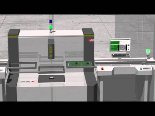
The X3 is an automatic X-Ray inspection system featuring combined Transmission and 3D Technology for sophisticated high-speed inspection in electronic production. The system is based on the motion concept of the MatriX X2.5 AXI system. A newly develo
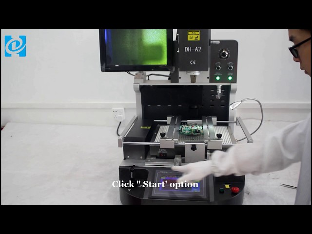
Dinghua Technology-- the leading manufacturer of BGA rework station, Automatic screw locking machine, Automatic soldering station and non-standard equipment. For more details, please just contact John, WhatsApp/Wechat:+86 1576811 4827 , Skype: si


