New Equipment | Fabrication Services
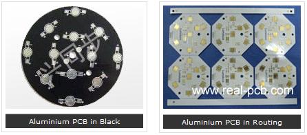
PCB Prototype to Volume Supplier in China - No Restriction in Order Quantity! REAL-PCB is a professional PCB supplier located in eastern coastal area of China, which is of all the convenient and efficient access to transportation and shipment. We p

New Equipment | Fabrication Services
PCB Prototype to Volume Supplier in China - No Restriction in Order Quantity! REAL-PCB is a professional PCB supplier located in eastern coastal area of China, which is of all the convenient and efficient access to transportation and shipment. We p
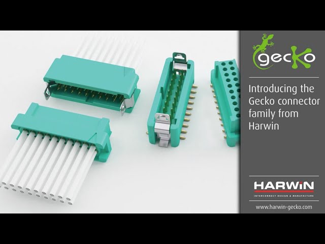
Harwin’s Gecko (G125 series) connectors provide a low profile, dual row cable-to-board and board-to-board interconnect solution, ideally suited for stacking and cable mating in areas where PCB real estate is at a premium. For more information and sa
Industry Directory | Manufacturer
The largest tin/lead secondary smelter in the western hemisphere, with a focus on recycling industrial metal waste streams. Areas of expertise include electronics dross, solder paste, solder wire, solder bar.
Industry Directory | Manufacturer
Nepes offers flip chip solutions ranging from wafer bumping to advanced packaging and testing for IC manufactures, module electronics and end-product makers.
Industry Directory | Manufacturer
Established in 2003,Shenzhen Keyou PCB Co. Ltd is a professional high-tech factory that is engaged in PCBs manufacturing,including high-precision double sided and multilayer circuit boards from China.
Industry News | 2023-09-04 13:25:54.0
Heraeus Electronics, an expert in materials and matched material solutions for the electronics packaging, is one of five partners in the three-year joint project "KuSIn - Copper sinter processes using induction heating for electromobility applications", funded by the German Federal Ministry of Economic Affairs and Climate Action (BMWK).
Industry News | 2019-11-05 22:08:21.0
Via in pad is the design practice of placing a via in the copper landing pad of a component. Compared to standard PCB via routing, via in pad allows a design to use smaller component pitch sizes and further reduce the PCBs overall size. With component manufactures pushing smaller parts every year and the demand from consumers for smaller devices, the usage of via in pad practices by hardware engineers have become more commonplace. In this article, we will discuss the differences between via in pad and traditional vias, when should you use via in pad, and how to design for it.
New Equipment | Solder Materials
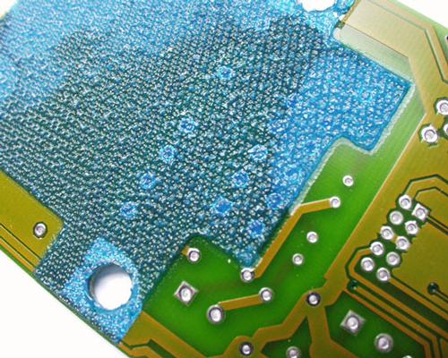
A variety of printed circuit boards require protection of selected board areas during the Surface Finish or Assembly Process. A wide range of PEELABLE SOLDER MASKS, the SD 295X Series including the popular SD 2954 and SD 2955 provide such protection
Technical Library | 2018-07-18 16:28:26.0
Reduction of first pass defects in the SMT assembly process minimizes cost, assembly time and improves reliability. These three areas, cost, delivery and reliability determine manufacturing yields and are key in maintaining a successful and profitable assembly process. It is commonly accepted that the solder paste printing process causes the highest percentage of yield challenges in the SMT assembly process. As form factor continues to get smaller, the challenge to obtain 100% yield becomes more difficult.This paper will identify defects affecting SMT yields in the printing process and discuss their Root Cause. Outer layer copper weight and surface treatment will also be addressed as to their effect on printability. Experiments using leadless and emerging components will be studied and root cause analysis will be presented


