Industry News | 2015-06-22 13:17:54.0
Insulectro (www.insulectro.com), a leading supplier of materials for use in the PCB and printed electronics industries, announced a breakthrough partnership to supply world-class performance copper foils manufactured by Oak-Mitsui throughout North America.
Industry Directory | Manufacturer
One of the largest manufacturers of interconnect products in the world. The company designs, and manufactures RF/microwave connectors; flat ribbon cable and interconnect systems.
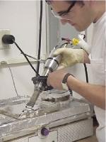
New Equipment | Assembly Services
S-Bond has been licensed as a supplier and provider of ultrasonic activated joining services using EWI SonicSolder®, an EWI patented* binary lead-free solder alloy that melts at 231°C. In conjunction with ultrasonic soldering, it can be used to join

By definition, anaerobic adhesives remain liquid until isolated from oxygen in the presence of metal ions, such as iron or copper. For example, when an anaerobic adhesive is sealed between a nut and a bolt on a threaded assembly, it rapidly "cures" o
Industry News | 2016-05-21 08:04:11.0
Oak-Mitsui are proud to announce an expanded strategic partnership adding Oak Mitsui’s proprietary ABC (aluminum bonded copper) to Insulectro’s premier product portfolio including CAC (copper aluminum copper). By leveraging their bicoastal manufacturing locations, ABC will continue to manufacture its bonded product in Hoosick Falls, NY and Insulectro will continue to manufacture CAC at its facility in Lake Forest, CA. The complete line of Oak-Mitsui copper foils, on CAC and ABC, will be available in Insulectro’s inventory by June 17, 2016.
Industry News | 2017-09-26 19:24:28.0
BTU International today announced that it will exhibit at Heat Treat, ASM’s Heat Treating Society Conference & Exhibition, scheduled to take place October 24-26, 2017 in Columbus, Ohio. BTU will highlight its controlled atmosphere furnaces in Booth #2524.
Industry News | 2020-02-01 05:21:42.0
BTU International is celebrating its 70-year anniversary. Since 1950, and with more than 10,000 units shipped, BTU International has been the trusted name for high-tech customers with a need to solve high-volume thermal processing challenges.
Industry News | 2012-05-30 13:50:20.0
Hesse & Knipps GmbH will discuss “Wedge Bonding for Chip-On-Board and Direct-Chip-Attach Applications” at the SMTA Philadelphia Chapter Meeting.
Technical Library | 2020-08-27 01:22:45.0
Initially adopted internal specifications for acceptance of printed circuit boards (PCBs) used for wire bonding was that there were no nodules or scratches allowed on the wirebond pads when inspected under 20X magnification. The nodules and scratches were not defined by measurable dimensions and were considered to be unacceptable if there was any sign of a visual blemish on wire-bondable features. Analysis of the yield at a PCB manufacturer monitored monthly for over two years indicated that the target yield could not be achieved, and the main reasons for yield loss were due to nodules and scratches on the wirebonding pads. The PCB manufacturer attempted to eliminate nodules and scratches. First, a light-scrubbing step was added after electroless copper plating to remove any co-deposited fine particles that acted as a seed for nodules at the time of copper plating. Then, the electrolytic copper plating tank was emptied, fully cleaned, and filtered to eliminate the possibility of co-deposited particles in the electroplating process. Both actions greatly reduced the density of the nodules but did not fully eliminate them. Even though there was only one nodule on any wire-bonding pad, the board was still considered a reject. To reduce scratches on wirebonding pads, the PCB manufacturer utilized foam trays after routing the boards so that they did not make direct contact with other boards. This action significantly reduced the scratches on wire-bonding pads, even though some isolated scratches still appeared from time to time, which caused the boards to be rejected. Even with these significant improvements, the target yield remained unachievable. Another approach was then taken to consider if wire bonding could be successfully performed over nodules and scratches and if there was a dimensional threshold where wire bonding could be successful. A gold ball bonding process called either stand-off-stitch bonding (SSB) or ball-stitch-on-ball bonding (BSOB) was used to determine the effects of nodules and scratches on wire bonds. The dimension of nodules, including height, and the size of scratches, including width, were measured before wire bonding. Wire bonding was then performed directly on various sizes of nodules and scratches on the bonding pad, and the evaluation of wire bonds was conducted using wire pull tests before and after reliability testing. Based on the results of the wire-bonding evaluation, the internal specification for nodules and scratches for wirebondable PCBs was modified to allow nodules and scratches with a certain height and a width limitation compared to initially adopted internal specifications of no nodules and no scratches. Such an approach resulted in improved yield at the PCB manufacturer.


