Industry News | 2023-05-03 09:01:22.0
Tresky GmbH from Hennigsdorf near Berlin will present its newly developed pre-sintering processes at this year's pcim EUROPE in Nuremberg. As assemblies with high-performance semiconductors represent a key technology for the global energy turnaround and electromobility, Tresky has been working on these manufacturing processes for some time and will present further product and process innovations in 2023 as part of additional development steps.
Industry News | 2022-01-18 15:17:42.0
BTU International, Inc. is pleased to announce the appointment of Chris Heesch as its new regional sales manager. Based out of California, he will cover the western US, as well as Mexico and Central America.
Industry News | 2014-12-12 12:24:17.0
PNC Inc. has obtained a new Horizontal Conveyorized CO-BRA BOND In-line Oxide Replacement line from IPS (Integrated Process Systems). The machine is capable of coating 100 panels per hour to help expedite the inner layer treatment process. Compared to the previous process of manual dip tanks, the Oxide Replacement line is far more efficient due to automation. By using fewer heaters, the new unit is more energy efficient as well.
Industry News | 2023-01-23 18:38:38.0
Heraeus Electronics returns to NEPCON Japan after two years of the pandemic. At the exhibition, which is scheduled to take place January 25-27, 2023, at The Tokyo Big Sight, Heraeus Electronics will bring a wide range of innovative materials to enhance power module and semiconductor device performance.
Industry News | 2010-06-04 17:36:28.0
DENVER — Krayden, Inc., a leading distributor of engineered materials, introduces the Permabond TA459 magnet adhesive that is non-corrosive to electrically conductive surfaces including copper.
Industry News | 2022-04-28 15:05:22.0
In times of climate change and increases in energy use, the demands of power modules for the efficient and reliable control of electric motors continue to rise. Modern module concepts are reaching their limits in terms of power density, current carrying capacity, and reliability to increase lifetime and reduce costs. A critical area for improving power modules is the material system used in them, as well as their electrical and thermal interconnection.
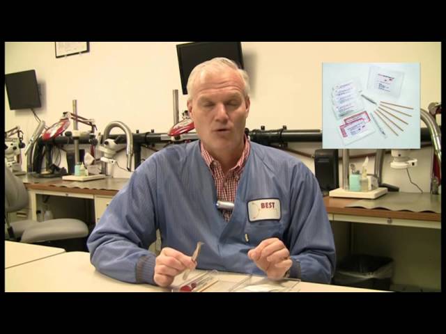
The BEST PCB pad repair repair kit gives you the tools you need for fast modification and repair of PCB circuit pads-no matter what their size. Our online PCB repair training videos, our master instructors along with these materials allows you to mee

PCB pad circuit repair using epoxy. Using multiple angles including overhead and from both right and left angles the BEST instructor staff demonstrates plainly how to repair a PCB pad using the epoxy method. This method is per IPC 7721 4.4.1. http://
Industry News | 2015-09-22 20:26:53.0
BTU International today announced that it will exhibit at Heat Treat 2015, ASM’s Heat Treating Society Conference & Exhibition, scheduled to take place Oct. 21-22, 2015, at the Cobo Convention Center in Detroit, MI. BTU will highlight its controlled atmosphere furnaces in Booth #449.
Industry News | 2016-07-20 16:44:36.0
BTU International today announced that it has received a repeat order from a North American-based customer for multiple PYRAMAX™ 125A units for LED assembly applications. PYRAMAX’s wide board capability and thermal uniformity were key factors in the purchase decision for the recent follow-on order.


