Industry News | 2018-10-18 11:08:03.0
Different Techniques for Plating
Technical Library | 2019-06-26 23:21:49.0
Copper-filled micro-vias are a key technology in high density interconnect (HDI) designs that have enabled increasing miniaturization and densification of printed circuit boards for the next generation of electronic products. Compared with standard plated through holes (PTHs) copper filled vias provide greater design flexibility, improved signal performance, and can potentially help reduce layer count, thus reducing cost. Considering these advantages, there are strong incentives to optimize the via filling process. This paper presents an innovative DC acid copper via fill formulation, for VCP (Vertical Continues Plating) applications which rapidly fills vias while minimizing surface plating.
Technical Library | 2021-11-03 17:05:39.0
Additively printed circuits provide advantages in reduced waste, rapid prototyping, and versatile flexible substrate choices relative to conventional circuit printing. Copper (Cu) based inks along with intense pulsed light (IPL) sintering can be used in additive circuit printing. However, IPL sintered Cu typically suffer from poor solderability due to high roughness and porosity. To address this, hybrid Cu ink which consists of Cu precursor/nanoparticle was formulated to seed Cu species and fill voids in the sintered structure. Nickel (Ni) electroplating was utilized to further improve surface solderability. Simulations were performed at various electroplating conditions and Cu cathode surface roughness using the multi-physics finite element method. By utilizing a mask during IPL sintering, conductivity was induced in exposed regions; this was utilized to achieve selective Ni-electroplating. Surface morphology and cross section analysis of the electrodes were observed through scanning electron microscopy and a 3D optical profilometer. Energy dispersive X-ray spectroscopy analysis was conducted to investigate changes in surface compositions. ASTM D3359 adhesion testing was performed to examine the adhesion between the electrode and substrate. Solder-electrode shear tests were investigated with a tensile tester to observe the shear strength between solder and electrodes. By utilizing Cu precursors and novel multifaceted approach of IPL sintering, a robust and solderable Ni electroplated conductive Cu printed electrode was achieved.
Industry Directory | Distributor / Manufacturer
Top 20 High-Quality PCB Fabrication and one-stop Turnkey PCB Assembly Facilities worldwide. Served national engineers for over 15 years, becoming a household name in providing full-feature multilayer PCBs engineers can trust.
Industry News | 2003-02-28 08:22:47.0
Dr. Zhang will lead the global R&D and product formulation activities of the company's tin, tin alloy and lead-free technologies.
With the development of miniaturization of assembly components, the layout area and pattern design area of PCBs have also been continuously reduced, and PCB manufacturers are constantly updating the production process to conform to the development tr
Technical Library | 2023-02-13 19:23:18.0
Spontaneously forming tin whiskers, which emerge unpredictably from pure tin surfaces, have regained prevalence as a topic within the electronics research community. This has resulted from the ROHS-driven conversion to "lead-free" solderable finish processes. Intrinsic stresses (and/or gradients) in plated films are considered to be a primary driving force behind the growth of tin whiskers. This paper compares the formation of tin whiskers on nanocrystalline and conventional polycrystalline copper deposits. Nanocrystalline copper under-metal deposits were investigated, in terms of their ability to mitigate whisker formation, because of their fine grain size and reduced film stress. Pure tin films were deposited using matte and bright electroplating, electroless plating, and electron beam evaporation. The samples were then subjected to thermal cycling conditions in order to expedite whisker growth. The resultant surface morphologies and whisker formations were evaluated.
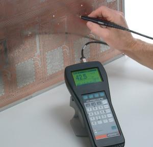
New Equipment | Test Equipment
The hand-held PHASCOPE® PMP10 is ideally suited for quality control in the electroplating and printed circuit board (PCB) industries. Because the instrument employs the phase-sensitive eddy current method (ISO 21 968), it allows the measurement of me
Technical Library | 2019-07-17 17:56:34.0
The increased demand for electronic devices in recent years has led to an extensive research in the field to meet the requirements of the industry. Electrolytic copper has been an important technology in the fabrication of PCBs and semiconductors. Aqueous sulfuric acid baths are explored for filling or building up with copper structures like blind micro vias (BMV), trenches, through holes (TH), and pillar bumps. As circuit miniaturization continues, developing a process that simultaneously fills vias and plates TH with various sizes and aspect ratios, while minimizing the surface copper thickness is critical. Filling BMV and plating TH at the same time, presents great difficulties for the PCB manufactures. The conventional copper plating processes that provide good via fill and leveling of the deposit tend to worsen the throwing power (TP) of the electroplating bath. TP is defined as the ratio of the deposit copper thickness in the center of the through hole to its thickness at the surface. In this paper an optimization of recently developed innovative, one step acid copper plating technology for filling vias with a minimal surface thickness and plating through holes is presented.
New Equipment | Test Equipment
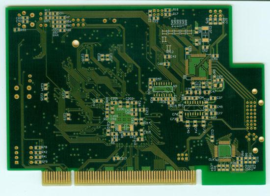
Printed Circuit Boards(PCBs) are used to electrically connect electronic components using conductive pathways, traces, etched from copper sheets laminated onto a non-conductive substrate. Our manufacturing processes utilise the latest techniques an


