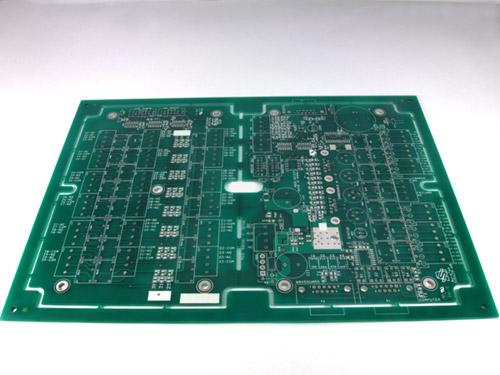
Standard Printed Circuit Boards custom manufactured over 1,000 double-sided, high-temperature printed circuit boards (PCBs) for a client from the Telecom/IT Industry. These PCBs are capable of withstanding continuous operating temperatures of 250° Ce
New Equipment | Assembly Services
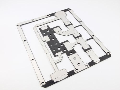
Heavy Copper Printed Circuits supplier Saturn Electronics Corp., bare printed circuit board manufacturer, was one of North America's largest users of heavy copper PCB laminate, which we used in the bare PCB manufacturing of Power Distribution Boards
Technical Library | 2015-11-12 19:04:51.0
In order to provide the functionality in today’s electronics, printed circuit boards are approaching the complexity of semiconductors. For flexible circuits with 1 mil lines and spaces, this means no nodules, no pits, and excellent ductility with thinner deposits. One of the areas that has to change to get to this plateau of technology is acid copper plating. Acid copper systems have changed in minor increments since their introduction decades ago. However, the basic cell design using soluble anodes in slabs or baskets has for the most part remained the same. Soluble, phosphorized, copper anodes introduce particulate and limits the ability to control plating distribution.
Technical Library | 2017-11-22 12:38:51.0
The use of copper foils laminated to polyimide (PI) as flexible printed circuit board precursor is a standard practice in the PCB industry. We have previously described[1] an approach to very thin copper laminates of coating uniform layers of nano copper inks and converting them into conductive foils via photonic sintering with a multibulb conveyor system, which is consistent with roll-to-roll manufacturing. The copper thickness of these foils can be augmented by electroplating. Very thin copper layers enable etching fine lines in the flexible circuit. These films must adhere tenaciously to the polyimide substrate.In this paper, we investigate the factors which improve and inhibit adhesion. It was found that the ink composition, photonic sintering conditions, substrate pretreatment, and the inclusion of layers (metal and organic) intermediate between the copper and the polyimide are important.

PCB pad circuit repair using epoxy. Using multiple angles including overhead and from both right and left angles the BEST instructor staff demonstrates plainly how to repair a PCB pad using the epoxy method. This method is per IPC 7721 4.4.1. http://
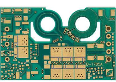
This PCB design utilizes surface mount technology Product Description This Double Sided Printed Circuit Board is a simple Surface Mount Technology PCB and is used within an Electronic Instrumentation Application Capabilities Applied/Processes Shea
Technical Library | 2020-03-26 14:55:29.0
This paper introduces line confocal technology that was recently developed to characterize 3D features of various surface and material types at sub-micron resolution. It enables automatic microtopographic 3D imaging of challenging objects that are difficult or impossible to scan with traditional methods, such as machine vision or laser triangulation.Examples of well-suited applications for line confocal technology include glossy, mirror-like, transparent and multi-layered surfaces made of metals (connector pins, conductor traces, solder bumps etc.), polymers (adhesives, enclosures, coatings, etc.), ceramics (components, substrates, etc.) and glass (display panels, etc.). Line confocal sensors operate at high speed and can be used to scan fast-moving surfaces in real-time as well as stationary product samples in the laboratory. The operational principle of the line confocal method and its strengths and limitations are discussed.Three metrology applications for the technology in electronics product manufacturing are examined: 1. 3D imaging of etched PCBs for micro-etched copper surface roughness and cross-sectional profile and width of etched traces/pads. 2. Thickness, width and surface roughness measurement of conductive ink features and substrates in printed electronics applications. 3. 3D imaging of adhesive dots and lines for shape, dimensions and volume in PCB and product assembly applications.
Technical Library | 2020-09-02 22:14:36.0
The demand for miniaturization and higher density electronic products has continued steadily for years, and this trend is expected to continue, according to various semiconductor technology and applications roadmaps. The printed circuit board (PCB) must support this trend as the central interconnection of the system. There are several options for fine line circuitry. A typical fine line circuit PCB product using copper foil technology, such as the modified semi-additive process (mSAP), uses a thin base copper layer made by pre-etching. The ultrathin copper foil process (SAP with ultrathin copper foil) is facing a technology limit for the miniaturization due to copper roughness and thickness control. The SAP process using sputtered copper is a solution, but the sputtering process is expensive and has issues with via plating. SAP using electroless copper deposition is another solution, but the process involved is challenged to achieve adequate adhesion and insulation between fine-pitch circuitries. A novel catalyst system--liquid metal ink (LMI)--has been developed that avoids these concerns and promotes a very controlled copper thickness over the substrate, targeting next generation high density interconnect (HDI) to wafer-level packaging substrates and enabling 5-micron level feature sizes. This novel catalyst has a unique feature, high density, and atomic-level deposition. Whereas conventional tin-palladium catalyst systems provide sporadic coverage over the substrate surface, the deposited catalyst covers the entire substrate surface. As a result, the catalyst enables improved uniformity of the copper deposition starting from the initial stage while providing higher adhesion and higher insulation resistance compared to the traditional catalysts used in SAP processes. This article discusses this new catalyst process, which both proposes a typical SAP process using the new catalyst and demonstrates the reliability improvements through a comparison between a new SAP PCB process and a conventional SAP PCB process.
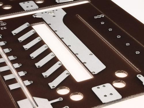
With a combination of specialized processes and equipment, the boards were custom manufactured from double-sided glass-reinforced PTFE. This PCB is used for controlled impedance within a microwave application.. Utilizing advanced photolithography a
Industry News | 2008-11-04 15:09:53.0
Saturn Electronics Corp. Heavy Copper Mulilayer Bare Boards


