Technical Library | 2020-09-02 22:02:13.0
With the adoption of Wafer Level Packages (WLP) in the latest generation mobile handsets, the Printed Circuit Board (PCB) industry has also seen the initial steps of High Density Interconnect (HDI) products migrating away from the current subtractive processes towards a more technically adept technique, based on an advanced modified Semi Additive Process (amSAP). This pattern plate process enables line and space features in the region of 20um to be produced, in combination with fully filled, laser formed microvias. However, in order to achieve these process demands, a step change in the performance of the chemical processes used for metallization of the microvia is essential. In the electroless Copper process, the critical activator step often risks cross contamination by the preceding chemistries. Such events can lead to uncontrolled buildup of Palladium rich residues on the panel surface, which can subsequently inhibit etching and lead to short circuits between the final traces. In addition, with more demands being placed on the microvia, the need for a high uniformity Copper layer has become paramount, unfortunately, as microvia shape is often far from ideal, the deposition or "throw" characteristics of the Copper bath itself are also of critical importance. This "high throwing power" is influential elsewhere in the amSAP technique, as it leads to a thinner surface Copper layer, which aids the etching process and enables the ultra-fine features being demanded by today's high end PCB applications. This paper discusses the performance of an electroless Copper plating process that has been developed to satisfy the needs of challenging amSAP applications. Through the use of a radical predip chemistry, the formation, build up and deposition of uncontrolled Pd residues arising from activator contamination has been virtually eradicated. With the adoption of a high throwing power Copper bath, sub 30um features are enabled and microvia coverage is shown to be greatly improved, even in complex via shapes which would otherwise suffer from uneven coverage and risk premature failure in service. Through a mixture of development and production data, this paper aims to highlight the benefits and robust performance of the new electroless Copper process for amSAP applications
Technical Library | 2020-07-22 19:39:05.0
The PWB industry needs to complete reliability testing in order to define the minimum copper wrap plating thickness requirement for confirming the reliability of PTH structures. Predicting reliability must ensure that the failure mechanism is demonstrated as a wear-out failure mode because a plating wrap failure is unpredictable. The purpose of this study was to quantify the effects of various copper wrap plating thicknesses through IST testing followed by micro sectioning to determine the failure mechanism and identify the minimum copper wrap thickness required for a reliable PWB. Minimum copper wrap plating thickness has become an even a bigger concern since designers started designing HDI products with buried vias, microvias and through filled vias all in one design. PWBs go through multiple plating cycles requiring planarization after each plating cycle to keep the surface copper to a manageable thickness for etching. The companies started a project to study the relationship between Copper wrap plating thickness and via reliability. The project had two phases. This paper will present findings from both Phase 1 and Phase 2.
New Equipment | Test Equipment
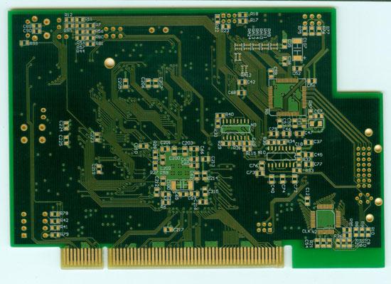
Printed Circuit Boards(PCBs) are used to electrically connect electronic components using conductive pathways, traces, etched from copper sheets laminated onto a non-conductive substrate. Our manufacturing processes utilise the latest techniques an
Industry News | 2020-11-03 13:18:05.0
MacDermid Alpha Electronics Solutions announces the release of CircuEtch 200, a high performance anisotropic final etch for circuit formation in Semi-Additive and modified-Semi-Additive processes (SAP/mSAP) utilized in IC substrate and substrate-like HDI manufacturing.
With the development of miniaturization of assembly components, the layout area and pattern design area of PCBs have also been continuously reduced, and PCB manufacturers are constantly updating the production process to conform to the development tr
Industry News | 2012-04-09 13:45:59.0
As the electronics assembly industry evolves, printed circuit board (PCB) features and surface mount technology (SMT) components continue to get smaller and smaller. This miniaturization shrinks the process window at print, placement, and reflow, increasing the opportunities for defects.

Our most popular course is now available on the Web!!! The Semiconductor Processing Overview course is now available online. Sign up for this course today and learn at your own pace in the comfort of your home or office. During this dynamic online
Industry News | 2011-04-04 15:48:55.0
Executive Associate Dr. Karl H. Dietz, of Weiner International Associates has completed preparation of the tutorial "HDI, Fine Line Processing." This is the capstone of his new suite of tutorials and seminars for bare board and substrate fabrication.
Industry News | 2012-02-07 00:27:29.0
SMART Group will host a four-part Webinar series titled Guide to Modern Multilayer Manufacture Webinar. Part 1 will take place from 14.30-16.00 GMT on Tuesday, March 6, 2012.


