Technical Library | 2015-04-30 20:17:03.0
Higher-speed signal transmission is increasingly required on a printed circuit board to handle massive data in electronic systems. So, signal transmission loss of copper wiring on a printed circuit board has been studied. First, total signal loss was divided into dielectric loss and conductor loss quantitatively based on electromagnetic theory. In particular, the scattering loss due to surface roughness of copper foil has been examined in detail. And the usefulness of the copper foil with low surface roughness has been demonstrated.
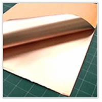
Designers and fabricators are always arguing about how to reduce track width and increase reliability of the circuitry. One effective solution is MicroThin�. MicroThin� is a very low profile copper 3�m or 5�m copper foil with an 18�m or 35�m peelable
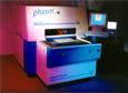
The phasor range of machines uses a different illumination and imaging technique and is designed for use with low contrast materials such as RTF, DSTF or double treated copper foils. phasor systems use the florescent properties of the pcb laminate to
Industry News | 2015-06-22 13:17:54.0
Insulectro (www.insulectro.com), a leading supplier of materials for use in the PCB and printed electronics industries, announced a breakthrough partnership to supply world-class performance copper foils manufactured by Oak-Mitsui throughout North America.
Technical Library | 2017-11-22 12:38:51.0
The use of copper foils laminated to polyimide (PI) as flexible printed circuit board precursor is a standard practice in the PCB industry. We have previously described[1] an approach to very thin copper laminates of coating uniform layers of nano copper inks and converting them into conductive foils via photonic sintering with a multibulb conveyor system, which is consistent with roll-to-roll manufacturing. The copper thickness of these foils can be augmented by electroplating. Very thin copper layers enable etching fine lines in the flexible circuit. These films must adhere tenaciously to the polyimide substrate.In this paper, we investigate the factors which improve and inhibit adhesion. It was found that the ink composition, photonic sintering conditions, substrate pretreatment, and the inclusion of layers (metal and organic) intermediate between the copper and the polyimide are important.

Paramount Enterprises with a renowned brand PARENTNashik is an ISO 9001:2015 certified company, listed in major leading manufacturers, suppliers & exporters of resistance spot welding consumables, spares, weldparts in Nashik – India. PARENTNashik is
Technical Library | 2012-12-26 20:18:50.0
①Single side The basic flexible printed circuit board is used of substrate of single side pcb materials and coated coverlay after finishing printed. ②Double sided That is made of substrates of double sided printed circuit board with double surface coated coverlays after finishing printed. ③Single copper foil with double coverlays Single copper foil coated different coverlays with double surface after finishing printed. ④Air gap Laminating two single printed circuit board together with no glue and bare design to meet high flexibility requirements. ⑤Multilayer That is designed for three and above circuit layers by laminating single side printed circuit board or double sided printed circuit board. ⑥COF IC chips and electronic components are installed on the flexible circuit board directly. ⑦Rigid-Flexible PCB Combined to rigid PCB with supporting and flexible PCB with high flexibility.
A high speed micro via drilling system, the GS-600 incorporates a dual laser system for the highest throughput and hole quality. Capable of producing up to 900 holes/second, the hole diameters can range from 0.001" to 0.010". The GS-600 is compatib
Industry News | 2016-05-21 08:04:11.0
Oak-Mitsui are proud to announce an expanded strategic partnership adding Oak Mitsui’s proprietary ABC (aluminum bonded copper) to Insulectro’s premier product portfolio including CAC (copper aluminum copper). By leveraging their bicoastal manufacturing locations, ABC will continue to manufacture its bonded product in Hoosick Falls, NY and Insulectro will continue to manufacture CAC at its facility in Lake Forest, CA. The complete line of Oak-Mitsui copper foils, on CAC and ABC, will be available in Insulectro’s inventory by June 17, 2016.
Technical Library | 2020-09-02 22:14:36.0
The demand for miniaturization and higher density electronic products has continued steadily for years, and this trend is expected to continue, according to various semiconductor technology and applications roadmaps. The printed circuit board (PCB) must support this trend as the central interconnection of the system. There are several options for fine line circuitry. A typical fine line circuit PCB product using copper foil technology, such as the modified semi-additive process (mSAP), uses a thin base copper layer made by pre-etching. The ultrathin copper foil process (SAP with ultrathin copper foil) is facing a technology limit for the miniaturization due to copper roughness and thickness control. The SAP process using sputtered copper is a solution, but the sputtering process is expensive and has issues with via plating. SAP using electroless copper deposition is another solution, but the process involved is challenged to achieve adequate adhesion and insulation between fine-pitch circuitries. A novel catalyst system--liquid metal ink (LMI)--has been developed that avoids these concerns and promotes a very controlled copper thickness over the substrate, targeting next generation high density interconnect (HDI) to wafer-level packaging substrates and enabling 5-micron level feature sizes. This novel catalyst has a unique feature, high density, and atomic-level deposition. Whereas conventional tin-palladium catalyst systems provide sporadic coverage over the substrate surface, the deposited catalyst covers the entire substrate surface. As a result, the catalyst enables improved uniformity of the copper deposition starting from the initial stage while providing higher adhesion and higher insulation resistance compared to the traditional catalysts used in SAP processes. This article discusses this new catalyst process, which both proposes a typical SAP process using the new catalyst and demonstrates the reliability improvements through a comparison between a new SAP PCB process and a conventional SAP PCB process.


