Industry News | 2019-11-05 22:10:56.0
Many customers and electronic designers were asking questions about the aluminum-based board, today our chief technical official Luca Zhang shared the knowledge and experience to you.
New Equipment | Fabrication Services
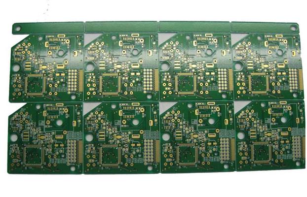
Low Cost Heavy Copper PCB China 4 Layers Circuit Boards Supplier Quick Details: FR4 base material 1.6mm board thickness 2oz heavy copper Plating gold finishing RF custom PCB boards Used for Radio Frequency From China PCB manufacturer Specifications
Industry News | 2012-01-13 12:42:50.0
Nihon Superior Co. Ltd., a supplier of advanced soldering materials to the global market, announces that Senior Technical Advisor Keith Sweatman will present “The Stability of Cu6Sn5 in the Formation and Performance of Lead-free Solder Joints” at the SMTA Pan Pacific Microelectronics Symposium.
Technical Library | 2021-11-03 16:52:47.0
This paper proposes the integration of pulsed photonic sintering into multi-material additive manufacturing processes in order to produce multifunctional components that would be nearly impossible to produce any other way. Pulsed photonic curing uses high power Xenon flash lamps to thermally fuse printed nanomaterials such as conductive metal inks. To determine the feasibility of the proposed integration, three different polymer additive manufacturing materials were exposed to typical flash curing conditions using a Novacentrix Pulseforge 3300 system. FTIR analysis revealed virtually no change in the polymer substrates, thus indicating that the curing energy did not damage the polymer. Next, copper traces were printed on the same substrate, dried, and photonically cured to establish the feasibility of thermally fusing copper metal on the polymer additive manufacturing substrates. Although drying defects were observed, electrical resistivity values ranging from 0.081 to 0.103 Ω/sq. indicated that high temperature and easily oxidized metals can be successfully printed and cured on several commonly used polymer additive manufacturing materials. These results indicate that pulsed photonic curing holds tremendous promise as an enabling technology for next generation multimaterial additive manufacturing processes.
Technical Library | 2017-11-22 12:38:51.0
The use of copper foils laminated to polyimide (PI) as flexible printed circuit board precursor is a standard practice in the PCB industry. We have previously described[1] an approach to very thin copper laminates of coating uniform layers of nano copper inks and converting them into conductive foils via photonic sintering with a multibulb conveyor system, which is consistent with roll-to-roll manufacturing. The copper thickness of these foils can be augmented by electroplating. Very thin copper layers enable etching fine lines in the flexible circuit. These films must adhere tenaciously to the polyimide substrate.In this paper, we investigate the factors which improve and inhibit adhesion. It was found that the ink composition, photonic sintering conditions, substrate pretreatment, and the inclusion of layers (metal and organic) intermediate between the copper and the polyimide are important.
Industry News | 2023-09-04 13:25:54.0
Heraeus Electronics, an expert in materials and matched material solutions for the electronics packaging, is one of five partners in the three-year joint project "KuSIn - Copper sinter processes using induction heating for electromobility applications", funded by the German Federal Ministry of Economic Affairs and Climate Action (BMWK).
New Equipment | Test Equipment
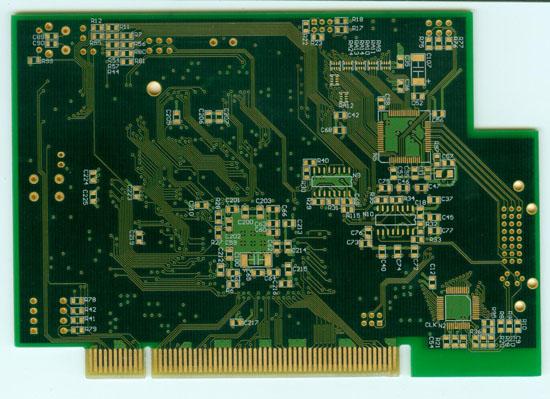
Printed Circuit Boards(PCBs) are used to electrically connect electronic components using conductive pathways, traces, etched from copper sheets laminated onto a non-conductive substrate. Our manufacturing processes utilise the latest techniques an
New Equipment | Assembly Services
We can bump single die in geometries as small as 30um. CVI will add a UBM on aluminum and copper pads follewed by solder bump in Sn and In alloys. CVI can then attach the die to a substrate or PCB followed by complete assembly.
New Equipment | Assembly Services
Benefit from our versatility and experience. We manufacture rigid printed circuit boards, rigid-flex and flexible printed circuit boards [including crimp technology]. You`ll find us flexible as far as dimensions are concerned: in addition to standard


