Technical Library | 2012-04-26 18:52:37.0
First presented at IPC Apex Expo 2012. The reliability, as tested by thermal cycling, of printed wire boards (PWB) are established by three variables; copper quality, material robustness and design. The copper quality was most influential and could be eva
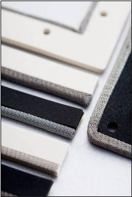
Knitted wire meshes are produced from a single continuous filament and produce very high levels of EMI shielding performance when evenly compressed between two metallic contact surfaces. Our KP Series meshes are available in four basic wire types –
Industry News | 2013-05-06 18:13:00.0
Hesse Mechatronics will offer application development, prototyping and pre-production services on a newly installed BONDJET BJ939 Fully Automatic Heavy Wire Bonder at the company’s west coast demonstration and applications lab, located at long-time company manufacturer's representative Chalman Technologies in Anaheim, California.
New Equipment | Solder Materials
KappAloy20™ - 80%Sn - 20%Zn For soldering of Aluminum to Aluminum and Aluminum to Copper. Good wetting. Used extensively in spray wire form for capacitors and other electronic parts. Higher temperature and higher tensile strength compared to 85Sn/15
Industry Directory | Manufacturer's Representative
Specialty materials for SMT Assembly. Solder Paste, Spheres, Tac Fluxes, Flip Chip Fluxes, Solder wi
Industry News | 2018-03-13 18:47:01.0
TopLine will once again be the premier sponsor of the upcoming IMAPS Wire Bonding Conference. In making the announcement, TopLine CEO Martin Hart stated that he is delighted to support the conference as the leading sponsor for the second time. The Wire Bonding workshop and tabletop exhibition will be held October 8, 2018 in California at the Pasadena Convention Center. The event is co-located with the IMAPS 51st Symposium on Microelectronics.

New Equipment | Test Equipment
ENGMATEC offers a range of test plugs for in-circuit and functional tests of standard industrial interfaces. The test plugs are designed to speed the production testing of electronic equipment incorporating a range of standard interfaces including
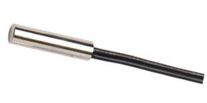
Copper tube NTC thermistor temperature sensor Application: Temperature measurement in air conditioner for regulating the evaporator temperature, and other HVAC (Heating, ventilation and air conditioning) application. Copper (brass) tube NTC thermi
Industry News | 2014-01-24 16:21:17.0
Hesse Mechatronics has appointed HTMG as the company's sales representative for South America.
Technical Library | 2020-08-27 01:22:45.0
Initially adopted internal specifications for acceptance of printed circuit boards (PCBs) used for wire bonding was that there were no nodules or scratches allowed on the wirebond pads when inspected under 20X magnification. The nodules and scratches were not defined by measurable dimensions and were considered to be unacceptable if there was any sign of a visual blemish on wire-bondable features. Analysis of the yield at a PCB manufacturer monitored monthly for over two years indicated that the target yield could not be achieved, and the main reasons for yield loss were due to nodules and scratches on the wirebonding pads. The PCB manufacturer attempted to eliminate nodules and scratches. First, a light-scrubbing step was added after electroless copper plating to remove any co-deposited fine particles that acted as a seed for nodules at the time of copper plating. Then, the electrolytic copper plating tank was emptied, fully cleaned, and filtered to eliminate the possibility of co-deposited particles in the electroplating process. Both actions greatly reduced the density of the nodules but did not fully eliminate them. Even though there was only one nodule on any wire-bonding pad, the board was still considered a reject. To reduce scratches on wirebonding pads, the PCB manufacturer utilized foam trays after routing the boards so that they did not make direct contact with other boards. This action significantly reduced the scratches on wire-bonding pads, even though some isolated scratches still appeared from time to time, which caused the boards to be rejected. Even with these significant improvements, the target yield remained unachievable. Another approach was then taken to consider if wire bonding could be successfully performed over nodules and scratches and if there was a dimensional threshold where wire bonding could be successful. A gold ball bonding process called either stand-off-stitch bonding (SSB) or ball-stitch-on-ball bonding (BSOB) was used to determine the effects of nodules and scratches on wire bonds. The dimension of nodules, including height, and the size of scratches, including width, were measured before wire bonding. Wire bonding was then performed directly on various sizes of nodules and scratches on the bonding pad, and the evaluation of wire bonds was conducted using wire pull tests before and after reliability testing. Based on the results of the wire-bonding evaluation, the internal specification for nodules and scratches for wirebondable PCBs was modified to allow nodules and scratches with a certain height and a width limitation compared to initially adopted internal specifications of no nodules and no scratches. Such an approach resulted in improved yield at the PCB manufacturer.


.gif)
