Events Calendar | Wed Sep 12 00:00:00 EDT 2018 - Sun Sep 30 00:00:00 EDT 2018 | ,
Improving Material Dispensing Yield in Manufacturing Applications
Industry News | 2014-04-10 10:17:27.0
AI Technology has just increased its manufacturing capacity to more than 10 million square feet of its 10 micron thick ESP7660 series of insulating DAF for memory stacked chip applications and its 20 micron thick ESP8660 series of conductive DAF for power devices.
Industry News | 2022-06-02 06:56:41.0
PVA is pleased to announce that it received a new patent in Japan for "optical bonding machine having cure in place and visual feedback." The new patent is based upon a machine and method designed specifically for applying a UV cure liquid optically clear adhesive used for bonding cover glass and/or sensors to touchscreens used most commonly in automotive, aerospace, military and medical applications. Key features covered by the patent are related to machine design and methods used.
Industry News | 2012-06-05 15:47:34.0
Engineered Material Systems introduces 535-10M-1 UV Cured Adhesive formulated for disk drive camera module, optoelectronic and circuit assembly applications.
Industry News | 2010-11-09 19:19:27.0
Krayden, Inc. debuts Dow Corning’s 3-6751 Thermally Conductive Adhesive used for bonding heat sinks to electronic devices and PCBs to substrates.
Technical Library | 2015-08-18 14:02:37.0
What is UV Curing? “Ultraviolet (UV) light is an electromagnetic radiation with a wavelength from 400 nm to 100 nm, shorter than that of visible light but longer than X-rays.” (Source: Wikipedia). Ultraviolet or UV curing is used to create a photochemical reaction using high intensity Ultraviolet (UV) energy or “light” to quickly dry inks, adhesives or conformal coatings. Most materials cure with a UV wavelength around 350 ~ 400nm although some materials require UVC energy near 255nm. There are many advantages to using UV curing over other traditional methods of curing. Not only will it increase production speed, it assists in creating a better bond, and improves scratch and solvent resistance. When compared to other methods of curing, UV curing generates a more reliable cured product at a much higher rate of production in a considerably shorter period of time.
Industry News | 2014-09-05 13:53:06.0
AI Technology, Inc (AIT) Develops Temporary Bonding Wax for Precision Wafer and Substrate Back-grinding and Thinning Applications. AI Technology, Inc. (AIT) has recently developed a series of temporary wax-like media that has been proven to be useful in many of these thinning applications.
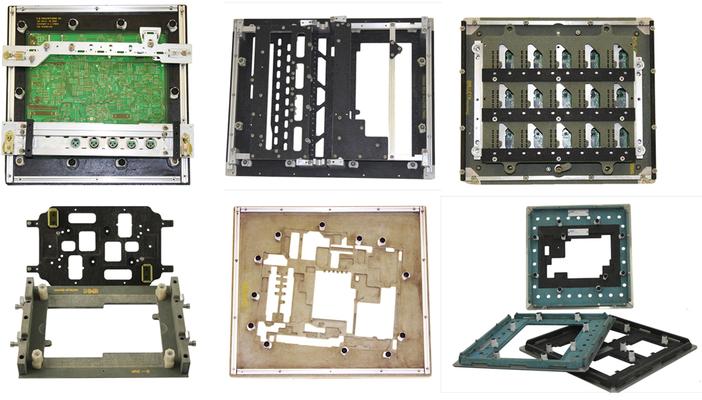
New Equipment | Board Handling - Pallets,Carriers,Fixtures
Our Wave Solder Fixtures increase productivity and eliminate defects in your pcb assembly process. This type of fixture supports the pcb on all four sides eliminating warpage that can cause solder skips and bridges or pcb flooding. They also elim
Technical Library | 2019-02-20 16:35:24.0
The High Density Packaging (HDP) User Group has completed a project evaluating the high frequency loss impacts of a variety of imaged core surface treatments (bond enhancement treatments, including chemical bonding and newer low etch alternative oxides) applied just prior to press lamination. Initial high frequency Dk/Df electrical test results did not show a strong correlation with any of the methods utilized within this project to measured surface roughness. The more significant factor affecting the measured loss is the choice of pre-lamination surface treatment. Most of the new chemical treatment systems outperform the older existing systems which depend upon surface roughness techniques to promote adhesion.
Industry News | 2011-01-18 13:46:21.0
Time and again, a major challenge lies in attaching integrated circuits (ICs) to highly integrated circuit board substrates in a space-saving manner. Würth Elektronik took this challenge on and found an ideal solution with the ESC (encapsulated solder connection) process. The chips are soldered and at the same time glued 'face-down" in their exact position.


