Industry News | 2012-09-17 16:02:44.0
Nordson DAGEa division of Nordson Corporation (NASDAQ: NDSN), announces that Dr. Evstatin Krastev, International Applications Engineering Manager, will present a paper titled “3D board level X-Ray inspection via Limited Angle Computer Tomography” at the upcoming SMTA International Conference & Exhibition
Industry News | 2010-05-20 13:24:15.0
HAMPSTEAD, N.H. - P.D. Circuits, Inc., specializing in delivering the highest quality PCBs, technical support, and service to OEM and EMS companies worldwide, announces that it has expanded its office staff in China in order to keep ahead of planned sales growth and to establish a broader role for the China office.
Industry News | 2011-06-07 15:07:59.0
P. D. Circuits announces the five-year anniversary of its Asian Operations Center, located in Shenzhen, China.
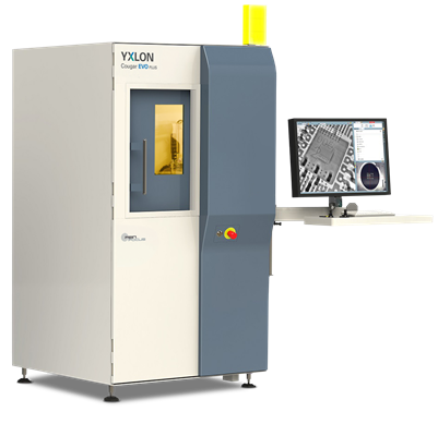
The YXLON Cougar EVO series was designed to provide the "best-in-class" inspection solutions for SMT, semiconductor, and laboratory assembly applications, while maintaining a small system footprint for maximum convenience. With optimized software and
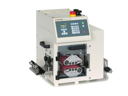
New Equipment | Cable & Wire Harness Equipment
Overview The PowerCut 3700 is the ideal solution for processing larger cable dimensions. It precisely cuts wire, round and flat cable, Glass Optical Fiber (GOF), tubing material, foil and more up to 70 mm² (AWG 2/0) and 25 mm (0.98 ") O.D. This auto
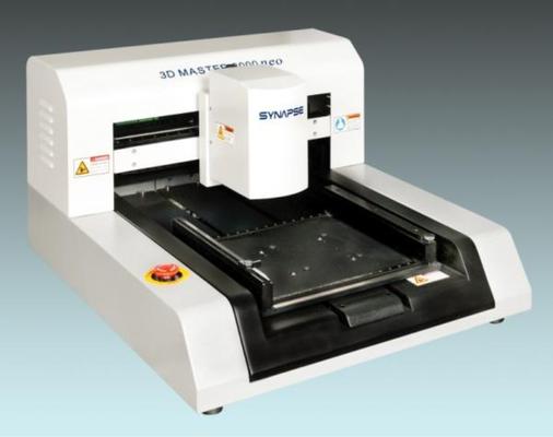
Description This device is designed to measure the shapes of 3-dimensional surfaces of objects that measure from dozen microns to a few millimeters, and is commonly used for measuring solder paste samples spread over PCBs automatically and 3-dimens
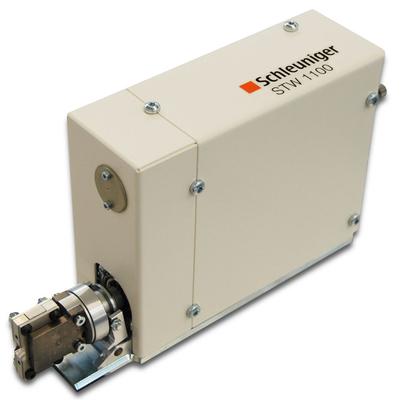
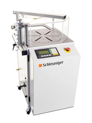
New Equipment | Cable & Wire Harness Equipment
Overview The STW 1100 twisting station is specifically designed for twisting conductor end strands with the fully automatic cut strip terminate machines of the CrimpCenter series. It easily handles wire sizes up to 2.5 mm² (14 AWG) and twists conduc
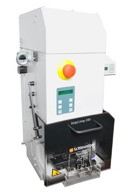
New Equipment | Cable & Wire Harness Equipment
Overview Get to know one of the most flexible stripper-crimper machines: The fully programmable StripCrimp 200. This machine is most suitable for high precision stripping and subsequent crimping of side- or rear-feed terminals for wires between 0.05
New Equipment | Cable & Wire Harness Equipment
Overview Heavy-duty single pan coiling system for in-line or stand-alone coiling of wire, cable or tubing. Coils cables up to an inner diameter of 300 mm (13") and handles coils weighing up to 40 kg (88 lbs.). It features a rotary design with movea


