Failure analysis - Components as well as PC boards, Discretes, Passives ICs - offering X-ray. SEM/EDX -XRF - Cross sectioning complete root cause F/A
Industry Directory | Consultant / Service Provider
Elmet LLC is an accredited lab, primarily providing cross sectioning of circuit boards, visual and x-ray inspections of PCBAs and other metallographic and metallurgical services including SEM examination and EDS analysis.

Double station Automatic PCB Router Machine for The Best Depaneling Solution Specification: Model CW-F01-S Standard working area 320*320mm(standard) Power 220V, 4.2KW Manipulator Repeatability ±0.

Features: This PCB Separator adopt x,y,z servo motor and driving system and ball screw ,linear guide rail ,ensure machine run smooth and precisely.moving accuracy less than 0.05mm, routing accuracy less then 0.05mm. Rotary do
Electronics Forum | Thu May 26 07:50:33 EDT 2011 | scottp
What process steps have been completed before the cross-section? What type of devices have solder cracks? Are the cracks found after just normal processing or after some type of validation testing? It is very unlikely to be a heating/cooling issue
Electronics Forum | Wed May 25 21:03:30 EDT 2011 | thanhnguyen22
Hi All, I am new the PCBA process fabrication. I have found many cracks in the PCB after we have cross sections analysis. The cracking has same kind of pattern. It happens betwen the solder and the PCB, or between the solder and the part, BUT not be
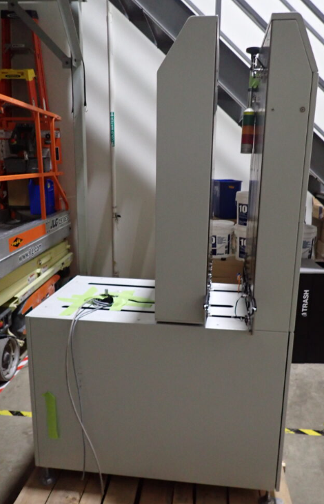
Used SMT Equipment | Conveyors
Description Make: FLEXLINK Model: F1200L Type: Board Handling Equipment Year: 2012 Details: In LIFO mode, the F1200 functions like a stack. The last board to be stored is the first board to be removed. This is useful for: Temporarily
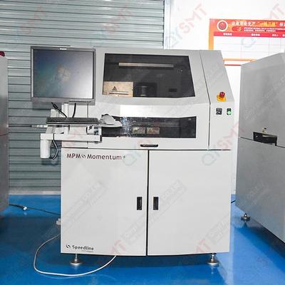
Used SMT Equipment | Screen Printers
Substrate processing: Maximum substrate size (XxY): 609.6mmx508mm(24”x20”) For circuit boards larger than 20”, special fixtures are required Minimum substrate size (XxY): 50.8mmx50.8mm(2”x2”)
Industry News | 2003-03-21 08:12:24.0
Tecan reckons it is consistently producing what may be regarded as the most efficient stencils in the world today.
Industry News | 2012-05-10 19:53:59.0
IPC is advocating changes to the draft SEC rule implementing Section 1502 of the Dodd-Frank Act that would lessen the burden on small manufacturing companies
Parts & Supplies | Pick and Place/Feeders
N210136905AB PLATE 0 N610124004AA フレキシブルコンベアステーション(搬送部)IPC対応 Flexible Conveyor St (Trannsport Unit) For IPC:NPM-D N210081910AB PLATE 0 N610087916AA 荷重キャリブレーションジグ Load Calibration Jig N210155534AA BRACKET 0 N610073135AA 交換台車切替ユニットガイド部:NPM Feeder
Parts & Supplies | Pick and Place/Feeders
N210095370AA COVER 0 KXFB0AU3A00 POST 0 KXF0E0NMA00 PLUG CP-30-HP-1 N210046856AA BRACKET 0 N510017083AA SPACER BSF-430E N510018125AA SCREW Cross recessed Countersunk head machine screw M2.5X8-4.8 A2J (Trivalen N210028733AA PLATE 0 KXFX064BA00
Technical Library | 2010-01-13 12:34:10.0
Micro-sectioning (sometimes referred to as cross-sectioning)is a technique, used to characterize materials or to perform a failure mode analysis, for exposing an internal section of a PCB or package. Destructive in nature, cross-sectioning requires encapsulation of the specimen in order to provide support, stability, and protection. Failures that can be investigated through micro-sectional analysis include component defects, thermo-mechanical failures, processing failures related to solder reflow, opens or shorts, voiding and raw material evaluations.
Technical Library | 2021-09-21 20:20:22.0
The electronics industry has been using the epoxy puck for the processing of the vast majority of electronics microsections since the 1970s. Minimal advancements have been seen in the methods used for precision micro-sections of PCBs, PCBAs, and device packages. This paper will discuss different techniques and approaches in performing precision and analytical micro-sections, which fuse the techniques and materials common in preparation of silicon wafers and bulk materials. These techniques have not only been found to produce excellent optical results, but transfer effectively to SEM for high magnification inspection and further analysis with minimal post-lapping preparation needed. Additionally, processing time is reduced primarily due to a significant reduction of bulk material removal earlier in the preparation, therefore needing less removal at later lapping steps compared to traditional sectioning methods. Additional techniques are introduced that mitigate some classic challenges experienced by technicians over the decades.
Events Calendar | Tue Jul 18 00:00:00 EDT 2023 - Tue Jul 18 00:00:00 EDT 2023 | Chippewa Falls, Wisconsin USA
UMW Chapter In-Person Event: PCB 101 Workshop and Tour at TTM Chippewa Falls
Events Calendar | Thu Aug 23 00:00:00 EDT 2018 - Thu Aug 23 00:00:00 EDT 2018 | ,
Strain Gauge Data Can Be Misleading | Predicting Strain Levels Caused by Mounting PCBs in Housing Using the ICT Analysis Feature of Sherlock
Career Center | Reynosa, Mexico | Engineering
This position is in our Reynosa manufacturing facility, which is across the border from McAllen, Texas. In this critical role, you will be responsible for PCBA, SMT, THT, Wave Solder and secondary operations which will include: =Ensure producti
Career Center | Williamsport, Pennsylvania USA | Engineering,Quality Control
Spartronics is a leader in complex electronics manufacturing and design services, serving customers in defense, aerospace, space, medical device, instrumentation & control, and life science markets. Spartronics is growing rapidly with manufacturi
Career Center | Alexandria, Egypt | Engineering,Maintenance,Management,Technical Support
I am an adaptable and fast learner person, I have an experience of 5 years at manufacturing and management of people, a good team player who can communicate with others to get and give the best he can for the working place, I want to develop my self
Career Center | Rochester, New York USA | Engineering
I have done my undergraduate studies in Mechanical Engineering. I am pursuing my Master's Program in Electronics Packaging. I am currently working as a Research Assistant for RIT-CEMA (Center for Electronics Manufacturing and Assembly). My research
Surface Mount Technology Association (SMTA) | https://www.smta.org/iceet/workshops.cfm
Plan view Through-scan Thermography Decapsulation Micro-probing Liquid crystal Emission microscopy Front side Back side Micro-sections SEM imaging Plan view Cross-sections EDX analysis Less common but useful
Heller 公司 | http://hellerindustries.com.cn/Vacuum-Void-Reduction-Reflow.pdf
(thermal fatigue reliability) by 23%. The photomicrographs taken from orthogonal cross sections of failed thermal cycling samples show that microvoiding and its effects on crack propagation are not always evident or easy to detect using


