Industry Directory | Manufacturer's Representative
Specialty materials for SMT Assembly. Solder Paste, Spheres, Tac Fluxes, Flip Chip Fluxes, Solder wi
Industry Directory | Manufacturer
Hermetic Power Package, Hermetic fiber optic package, Sensor Header, Hermetic IC Hyrbid packge, TO Header
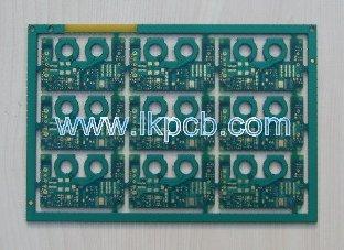
FR-4 Material 2. 4 mm Thickness 3OZ base Cu 10 Layers Immersion Gold Surface Treatment Green Solder Mask

Layer: Single-Sided Price:USD275.50 Quantity :3Panel Min Holes:2.00mm surface Treatment:ENIG solder mask:White silk screen : Black Board Thickness: 1.6mm Cu Thickness: 35um Aluminium Model: 5052 Thermal Conductivity: 150W/m. K Breakdown Voltage:
Electronics Forum | Fri Oct 03 05:27:24 EDT 2003 | kanwal324
the puspose of solder mask is to prevent exposure of cu tracks to atmosphere. the lesser thickness can effect the performance of board but it only depends on its application. if you are making telecom board then its not good to use the board.
Electronics Forum | Wed Nov 17 10:03:29 EST 2010 | scottp
Instead of a minimum thickness, we require no exposed copper or SnCu intermetallic. We've been having a lot of trouble lately with suppliers of SN100 HASL boards giving us pads with very irregular solder deposits with areas of exposed intermetallic.
Used SMT Equipment | Semiconductor & Solar
Standard Machine features and system description: Ultra-fine pitch and small ball bonding capabilities High frequency transducer operating at 138 kHz Applicable wire size of 0.6mil-2.0mil High speed XY table with linear motor technology High ac
Industry News | 2010-05-30 23:23:13.0
Minneapolis, MN - The Surface Mount Technology Association (SMTA) announces the Call for Papers for the 2011 Pan Pacific Microelectronics Symposium, which will be held January 18-20, 2011 on the Big Island of Hawaii. The symposium focuses on the critical business markets and technologies of microelectronic packaging, interconnection, microsystems technology and assembly. The deadline for abstracts is July 16, 2010.
Industry News | 2010-08-17 13:31:00.0
The Pan Pacific Microelectronics Symposium promotes International technical interchange and provides a premier forum for extensive networking among microelectronics professionals and business leaders throughout the Pacific Basin. Participants come from Australia, China, India, Japan, Korea, North America, Southeast Asia, and Taiwan as well as Europe!
Parts & Supplies | General Purpose Equipment
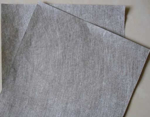
Our conductive non-woven fabric is plated Cu+Ni on non-woven fabric,it has good conductivity and shielding effectiveness,it is widely used in various electronic products.The thickness of our non-woven fabric is 0.035mm,0.045mm,0.04mm,0.08mm,0.10mm,0.
Technical Library | 2010-04-29 21:40:37.0
The purpose of this paper is to investigate the effects of reflow time, reflow peak temperature, thermal shock and thermal aging on the intermetallic compound (IMC) thickness for Sn3.0Ag0.5Cu (SAC305) soldered joints.
Technical Library | 2014-07-02 16:46:09.0
Growth behaviors of intermetallic compounds (IMCs) and Kirkendall voids in Cu/Sn/Cu microbump were systematically investigated by an in-situ scanning electron microscope observation. Cu–Sn IMC total thickness increased linearly with the square root of the annealing time for 600 h at 150°C, which could be separated as first and second IMC growth steps. Our results showed that the growth behavior of the first void matched the growth behavior of second Cu6Sn5, and that the growth behavior of the second void matched that of the second Cu3Sn. It could be confirmed that double-layer Kirkendall voids growth kinetics were closely related to the Cu–Sn IMC growth mechanism in the Cu/Sn/Cu microbump, which could seriously deteriorate the mechanical and electrical reliabilities of the fine-pitch microbump systems
With the development of miniaturization of assembly components, the layout area and pattern design area of PCBs have also been continuously reduced, and PCB manufacturers are constantly updating the production process to conform to the development tr

SMTnet Express, June 20, 2019, Subscribers: 32,068, Companies: 10,815, Users: 24,854 Dissolution in Service of the Copper Substrate of Solder Joints Credits: Nihon Superior Co., Ltd. It is well known that during service the layer of Cu6Sn5
Influence of Pd Thickness on Micro Void Formation of Solder Joints in ENEPIG Surface Finish SMTnet Express December 13, 2012, Subscribers: 26067, Members: Companies: 9068, Users: 34058 Influence of Pd Thickness on Micro Void Formation of Solder
| https://www.eptac.com/wp-content/uploads/2012/10/eptac_11_14_12.pdf
ASYMTEK Products | Nordson Electronics Solutions | https://www.nordson.com/en/divisions/dage/technical-experts/2d-x-ray-inspection
. Figure 9. Illustration of how the MAP technology can be used to measure precise Cu track thickness information. This can be used to generate thickness profiles (top right) or a full three dimensional representation of the copper thickness across the PCB


.gif)


