_1.jpg)
Parts & Supplies | Chipshooters / Chip Mounters
QC Process ZK Electronic is an Electronic components distributor. We have supported global customers' business with our high-quality products and service. To match customers' requirements, our QC Team will conduct a complete inspection of all the p
Industry Directory | Consultant / Service Provider / Manufacturer
TDM International is a supplier of expert GenRad 228x and Teradyne TestStation test engineering services and quality test fixtures.
Industry News | 2019-11-05 22:07:01.0
Tenting a via refers to covering via with soldermask to enclose or skin over the opening. A via is a hole drilled into the PCB that allows multiple layers on the PCB to be connected to each other. A non tented via is just a via that is not covered with the soldermask layer. Leaving these vias exposed or covered has pros and cons depending on the your design and manufacturing requirements.
New Equipment | Cable & Wire Harness Equipment
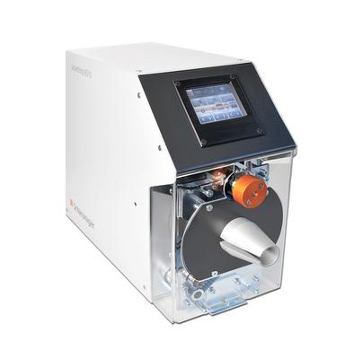
Overview The JacketStrip 8310 axially and radially slits the insulation of out-of-round and multi-conductor cables from 2.5 - 25 mm (0.1" - 1'') O.D. and up to 500 mm (19.7") in stripping length without any damage to the inner conductors or shieldin
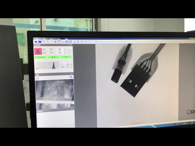
This video presents how to replace and inspect BGA on PCB with our BGA rework station R720 & X ray inspection machine X6600. More details, pls contact me: WhatsApp?+86 18779975930 Skype?joyrongzhuomao@outlook.com Email: sales25@zhuomao.com.cn Link
This video presents how to replace and inspect BGA on PCB with our BGA rework station R720 & X ray inspection machine X6600. More details, pls contact me: WhatsApp?+86 18779975930 Skype?joyrongzhuomao@outlook.com Email: sales25@zhuomao.com.cn Link
This video presents how to replace and inspect BGA on PCB with our BGA rework station R720 & X ray inspection machine X6600. More details, pls contact me: WhatsApp?+86 18779975930 Skype?joyrongzhuomao@outlook.com Email: sales25@zhuomao.com.cn Link

The JacketStrip 8310 axially and radially slits the insulation of out-of-round and multi-conductor cables from 0.1" - 1'' (2.5 - 25 mm) O.D. and up to 19.7" (500 mm) in stripping length without any damage to the inner conductors or shielding.
Industry Directory | Manufacturer
Buyers of Scrap Materials and Surplus Machinery, Equipment and Inventories Precious Metal Refining Warehouse Liquidation PCB & Electronic Scrap Recycling Purchasing of Used Surplus Semiconductor
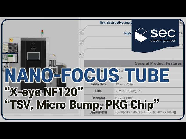
#Xray#Inspection#SEC Nano-focus Tube of 200 nano resolution which is specialized for sub-micron defects of Semiconductor Packaging, Wafer Level Packaging(WLP). -Non-destructive Analysis System -High-Resolution Image with Dual Type CTs -Application


.png)


