Technical Library | 2023-07-25 16:25:56.0
This paper address two significant applications of stencils in advance packaging field: 1. Ultra-Thin stencils for miniature component (0201m) assembly; 2. Deep Cavity stencils for embedded (open cavity) packaging. As the world of electronics continues to evolve with focus on smaller, lighter, faster, and feature-enhanced high- performing electronic products, so are the requirement for complex stencils to assemble such components. These stencil thicknesses start from less than 25um with apertures as small as 60um (or less). Step stencils are used when varying stencil thicknesses are required to print into cavities or on elevated surfaces or to provide relief for certain features on a board. In the early days of SMT assembly, step stencils were used to reduce the stencil thickness for 25 mil pitch leaded device apertures. Thick metal stencils that have both relief-etch pockets and reservoir step pockets are very useful for paste reservoir printing. Electroform Step-Up Stencils for ceramic BGA's and RF Shields are a good solution to achieve additional solder paste height on the pads of these components as well as providing exceptional paste transfer for smaller components like uBGAs and 0201s. As the components are getting smaller, for example 0201m, or as the available real estate for component placement on a board is getting smaller – finer is the aperture size and the pitch on the stencils. Aggressive distances from step wall to aperture are also required. Ultra-thin stencils with thicknesses in the order of 15um-40um with steps of 15um are used to obtain desired print volumes. Stencils with thickness to this order can be potential tools even to print for RDLs in the package.
Industry Directory | Equipment Dealer / Broker / Auctions
FabExchange uses our extensive global connections to source the best tools and buyers for semiconductor manufacturing equipment. Our unique combination of brokerage and auction services equips us to execute on any project.
New Equipment | Board Handling - Storage
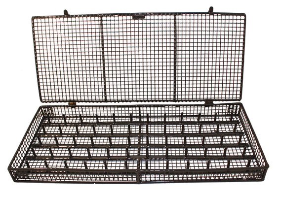
Baskets can be designed for your special needs. This low cost custom basket with an ESD safe coating to protect your parts in a batch cleaning or in-line cleaning process. Test Chambers PCB rack for test chambers. Withs
New Equipment | Fabrication Services
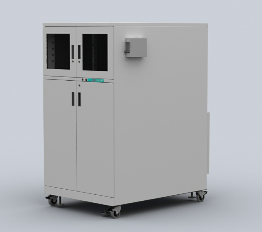
Custom Built F 54 Inch our Deep Largest Feeder cabinet ! Features : Modular design: : modularly designed dry cabinet. The main modules include dry units, control box, sensor, shelves and castors. • our cabinets use the h
Industry News | 2014-10-13 18:17:46.0
ADLINK Technology announced the opening of demo room developed in collaboration with Intel at ADLINK's Shanghai Operations Center as the kick-off event for a newly-signed collaborative technology strategy. Combining Intel's latest development technologies with ADLINK's established design capabilities, this new era of cooperation promises to deliver advanced, cutting-edge switching, transcoding, and deep packet inspection solutions for the next iteration of the intelligent edge cloud computing platform.
Industry News | 2018-10-18 20:53:18.0
This year at electronica Seica will be showing the power and performance of the new VIVA Next hardware and software platform in a totally innovative setting: a virtual factory, where visitors will be able to explore, hands-on, inside and out, Seica's Pilot V8 flying probe tester, as well as view the fully automated Compact SL for in-circuit and functional test and the Firefly Next, Seica's cutting-edge, laser-based selective soldering system.
eInnoSys staff has decades of extensive experience in Fab Automation of varying size and kind – from 4 inch GaAs or another compound semiconductor to 300 mm Silicon fabs as well as Packaging, Test/Assembly factories. Our team members have helpe
Industry News | 2023-01-18 11:19:25.0
Vista, CA – January 18, 2023. Machine Vision Products, Inc (MVP) will be exhibiting on booth 924 at the IPC Apex Expo 2023 in the San Diego Convention Center between January 24-26.
Vision Engineering unveils ‘Game Changing’ 3D digital display technology Vision Engineering Inc.launches revolutionary, globally patented, digital 3D stereoscopic display technology for inspection and design & development applicatio
Industry News | 2020-07-22 04:00:43.0
OUR FULL TEST LINE SOLUTION FOR REEL TO REEL MARKET


