Industry News | 2007-12-07 14:15:38.0
This year�s Productronica exhibition saw DEK showcase its Expect More philosophy through a range of global product launches and exciting live technology demonstrations. The result was a highly successful exhibition for the whole DEK team, reinforced by the two trophies the mass imaging leader picked up at the Global Technology Awards.
Industry News | 2012-03-21 17:06:11.0
At the APEX event held earlier this month, DEK proudly accepted its tenth consecutive Service Excellence Award,
Systronix, Inc. is an industry leader in the supply of electronic manufacturing services. We provide a broad range of services to leading companies in industries that require high tech, high quality and highly reliable electronics.
Industry News | 2009-06-02 14:19:00.0
Further extending its world-class stencil manufacturing capabilities, DEK announces that the company has applied for and been granted official International Traffic in Arms Regulations (ITAR) registration. This status enables the mass imaging pioneer to actively engage in the manufacture and sale of military-related stencil products, effectively broadening DEK's comprehensive range of stencil portfolio offerings.
Industry News | 2008-04-09 14:30:19.0
For electronics industry specialists who want the most advanced and cost-effective materials deposition technologies available, DEK is a sure bet. Over the three days at APEX in Las Vegas last week, DEK�s leadership position was again confirmed as the mass imaging front runner earned three top industry honors.
Industry News | 2010-06-04 17:55:16.0
DEK has appointed SmartRep to distribute its high accuracy mass imaging technologies in Germany, extending product accessibility and support opportunities for customers in South Germany.
Industry News | 2009-11-29 22:25:49.0
Showcasing the latest expansion of its global stencil network, DEK and new franchisee, Huntsville, Alabama-based AGI Corporation, opened the doors of their manufacturing operation to local customers on October 21, 2009. Attended by both leading EMS and OEM electronics firms as well as Huntsville’s Mayor, Mr. Tommy Battle, the DEK-AGI Open House was a technology-rich event designed to highlight the company’s stencil production expertise.
Advanced semiconductor packaging and high precision SMT assembly convergence. Galaxy unites advanced semiconductor packaging and high precision next-generation SMT assembly on the same platform. This level of convergence delivers the advanced techno
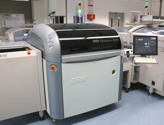
Used SMT Equipment | Screen Printers
Ready to use. DEK Horizon 03iX 2014 email at sidarcv@gmail.com In-line automatic printing machine - Dimensions : 1314 x 1601 x 1486 mm - Weight : 760 Kg - PCB max. dimensions : 508.5 x 508.5 mm - PCB min. dimensions : 50 x 40.5 mm - PCB th
Industry News | 2009-07-16 14:40:44.0
DEK Solar will use this year’s EU PVSEC exhibition to reveal how standard print processes can be developed to yield dramatic efficiency gains. Being held over September 21st – 25th in Hamburg, Germany, the show will see DEK Senior Process Development Specialist Tom Falcon present a new paper on aspect ratio improvements for printed frontside conductors on silicon solar cells.


